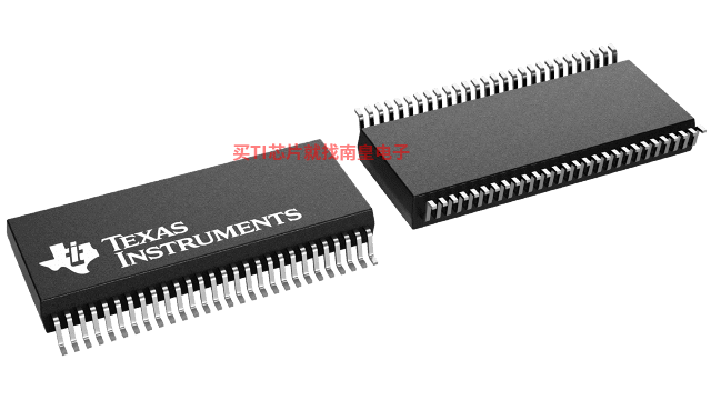
- 制造厂商:TI
- 产品类别:逻辑和电压转换
- 技术类目:缓冲器、驱动器和收发器 - 通用收发器
- 功能描述:具有奇偶校验发生器/校验器和三态输出的 16 位收发器
- 点击这里打开及下载74ACT16657的技术文档资料
- TI代理渠道,提供当日发货、严格的质量标准,满足您的目标价格

The 'ACT16657 contain two noninverting octal transceiver sections with separate parity generator/checker circuits and control signals. For either section, the transmit/receive (1T/R\ or 2T/R\) input determines the direction of data flow. When 1T/R\ (or 2T/R\) is high, data flows from the 1A (or 2A) port to the 1B (or 2B) port (transmit mode); when 1T/R\ (or 2T/R\) is low, data flows from the 1B (or 2B) port to the 1A (or 2A) port (receive mode). When the output-enable (1![]() or 2
or 2![]() ) input is high, both the 1A (or 2A) and 1B (or 2B) ports are in the high-impedance state.
) input is high, both the 1A (or 2A) and 1B (or 2B) ports are in the high-impedance state.
Odd or even parity is selected by a logic high or low level, respectively, on the 1ODD/![]() (or 2ODD/
(or 2ODD/![]() ) input. 1PARITY (or 2PARITY) carries the parity bit value; it is an output from the parity generator/checker in the transmit mode and an input to the parity generator/checker in the receive mode.
) input. 1PARITY (or 2PARITY) carries the parity bit value; it is an output from the parity generator/checker in the transmit mode and an input to the parity generator/checker in the receive mode.
In the transmit mode, after the 1A (or 2A) bus is polled to determine the number of high bits, 1PARITY (or 2PARITY) is set to the logic level that maintains the parity sense selected by the level at the 1ODD/![]() (or 2ODD/
(or 2ODD/![]() ) input. For example, if 1ODD/
) input. For example, if 1ODD/![]() is low (even parity selected) and there are five high bits on the 1A bus, then 1PARITY is set to the logic high level so that an even number of the nine total bits (eight 1A-bus bits plus parity bit) are high.
is low (even parity selected) and there are five high bits on the 1A bus, then 1PARITY is set to the logic high level so that an even number of the nine total bits (eight 1A-bus bits plus parity bit) are high.
In the receive mode, after the 1B (or 2B) bus is polled to determine the number of high bits, the 1![]() (or 2
(or 2![]() ) output logic level indicates whether or not the data to be received exhibits the correct parity sense. For example, if 1ODD/
) output logic level indicates whether or not the data to be received exhibits the correct parity sense. For example, if 1ODD/![]() is high (odd parity selected), 1PARITY is high, and there are three high bits on the 1B bus, then 1
is high (odd parity selected), 1PARITY is high, and there are three high bits on the 1B bus, then 1![]() is low, indicating a parity error.
is low, indicating a parity error.
The 74ACT16657 is packaged in TI's shrink small-outline package, which provides twice the I/O pin count and functionality of standard small-outline packages in the same printed-circuit-board area.
The 54ACT16657 is characterized for operation over the full military temperature range of -55°C to 125°C. The 74ACT16657 is characterized for operation from -40°C to 85°C.
- Members of the Texas Instruments WidebusTM Family
- Inputs Are TTL-Voltage Compatible
- Flow-Through Architecture Optimizes PCB Layout
- Distributed VCC and GND Pin Configuration Minimizes High-Speed Switching Noise
- EPICTM (Enhanced-Performance Implanted CMOS) 1-m Process
- 500-mA Typical Latch-Up Immunity at 125°C
- Package Options Include Plastic 300-mil Shrink Small-Outline (DL) Packages Using 25-mil Center-to-Center Pin Spacings and 380-mil Fine-Pitch Ceramic Flat (WD) Packages Using 25-mil Center-to-Center Pin Spacings
EPIC and Widebus are trademarks of Texas Instruments Incorporated.
- IOL (Max) (mA)
- 24
- IOH (Max) (mA)
- -24
- Technology Family
- ACT
- Rating
- Catalog
- Operating temperature range (C)
- -40 to 85
74ACT16657的完整型号有:74ACT16657DLR,以下是这些产品的关键参数及官网采购报价:
74ACT16657DLR,工作温度:-40 to 85,封装:SSOP (DL)-56,包装数量MPQ:1000个,MSL 等级/回流焊峰值温度:Level-1-260C-UNLIM,引脚镀层/焊球材料:NIPDAU,TI官网74ACT16657DLR的批量USD价格:6.729(1000+)

74ACT16657DLR,工作温度:-40 to 85,封装:SSOP (DL)-56,包装数量MPQ:1000个,MSL 等级/回流焊峰值温度:Level-1-260C-UNLIM,引脚镀层/焊球材料:NIPDAU,TI官网74ACT16657DLR的批量USD价格:6.729(1000+)


