- 制造厂商:TI
- 产品类别:数据转换器
- 技术类目:模数转换器 (ADC) - 高速模数转换器 (>10MSPS)
- 功能描述:缓冲区容量为 1K 的 8 位、200MSPS 模数转换器 (ADC)
- 点击这里打开及下载ADC08B200的技术文档资料
- TI代理渠道,提供当日发货、严格的质量标准,满足您的目标价格

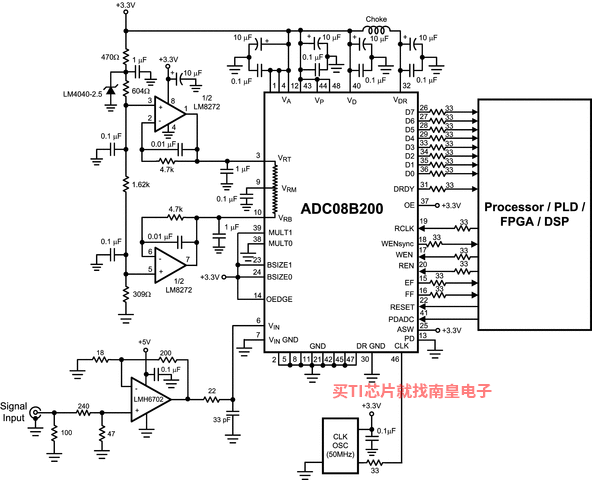
The ADC08B200 is a high speed analog-to-digital converter (ADC) with an integrated capture buffer. The 8-bit, 200 MSPS A/D core is based upon the proven ADC08200 with integrated track-and-hold and is optimized for low power consumption. This device contains a selectable size capture buffer of up to 1,024 bytes that allows fast capture of an input signal with a slower readout rate. An on-chip clock PLL circuit provides the option of on-chip clock rate multiplication to provide the high speed sampling clock.
The ADC08B200 is resistant to latch-up and the outputs are short-circuit proof. The top and bottom of the ADC08B200's reference ladder are available for connections, enabling a wide range of input possibilities. The digital outputs are TTL/CMOS compatible with a separate output power supply pin to support interfacing with 2.7V to 3.3V logic. The digital inputs and outputs are low voltage TTL/CMOS compatible and the output data format is straight binary.
The ADC08B200Q runs on an Automotive Grade Flow and is AEC-Q100 Grade 2 Qualified.
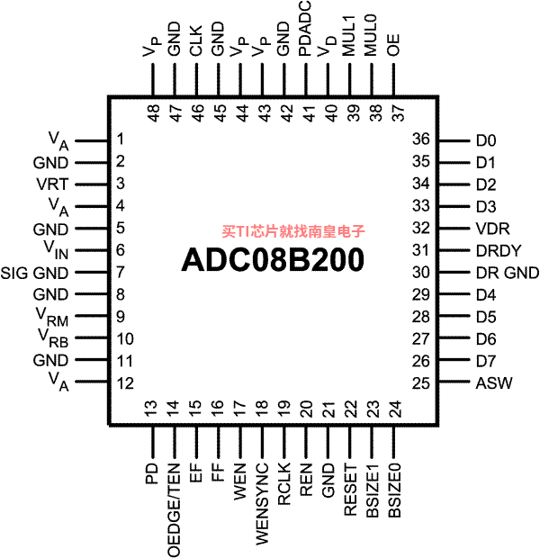
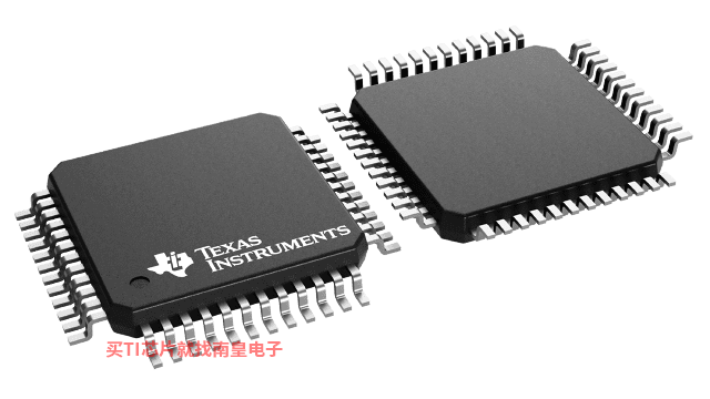
The ADC08B200 is offered in a 48-pin plastic package (TQFP) and is specified over the extended industrial temperature range of −40°C to +105°C. An evaluation board is available to assist in the easy evaluation of the ADC08B200.
- Single-Ended Input
- Selectable Capture Buffer Size
- PLL for Clock Multiplication
- Reference Ladder Top and Bottom Accessible
- Linear Power Scaling with Sample Rate
- FPGA Training Pattern
- AEC-Q100 Grade 2 Qualified
- Power-Down Feature
- Resolution 8 Bits
- Maximum Sampling Frequency 200 MSPS (min)
- DNL ±0.4 LSB (typ)
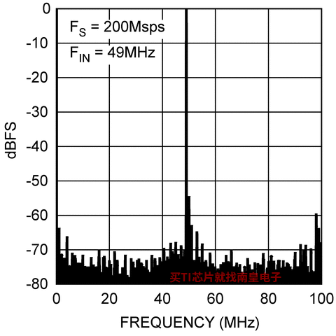
- ENOB (fIN= 49 MHz) 7.2 bits (typ)
- THD (fIN= 49 MHz) ?53 dBc (typ)
- Power Consumption
- Operating (50 MHz) Input 2 mW / Msps (typ)
- Power Down 2.15 mW (typ)
(PLL Bypassed)
All trademarks are the property of their respective owners.
- Sample rate (Max) (MSPS)
- 200
- Resolution (Bits)
- 8
- Number of input channels
- 1
- Interface type
- Parallel CMOS
- Analog input BW (MHz)
- 500
- Features
- Low Power
- Rating
- Catalog
- Input range (Vp-p)
- 1.6
- Power consumption (Typ) (mW)
- 543
- Architecture
- Pipeline
- SNR (dB)
- 47
- ENOB (Bits)
- 7.4
- SFDR (dB)
- 56
- Operating temperature range (C)
- -40 to 105
- Input buffer
- No
ADC08B200的完整型号有:ADC08B200CIVS/NOPB,以下是这些产品的关键参数及官网采购报价:
ADC08B200CIVS/NOPB,工作温度:-40 to 105,封装:TQFP (PFB)-48,包装数量MPQ:250个,MSL 等级/回流焊峰值温度:Level-3-260C-168 HR,引脚镀层/焊球材料:SN,TI官网ADC08B200CIVS/NOPB的批量USD价格:17.57(1000+)

PSPICE-FOR-TI ― 适用于 TI 设计和模拟工具的 PSpice
PSpice for TI 可提供帮助评估模拟电路功能的设计和仿真环境。此功能齐全的设计和仿真套件使用 Cadence 的模拟分析引擎。PSpice for TI 可免费使用,包括业内超大的模型库之一,涵盖我们的模拟和电源产品系列以及精选的模拟行为模型。借助?PSpice for TI 的设计和仿真环境及其内置的模型库,您可对复杂的混合信号设计进行仿真。创建完整的终端设备设计和原型解决方案,然后再进行布局和制造,可缩短产品上市时间并降低开发成本。
在?PSpice for TI 设计和仿真工具中,您可以搜索 TI (...)
