- 制造厂商:TI
- 产品类别:数据转换器
- 技术类目:模数转换器 (ADC) - 高速模数转换器 (>10MSPS)
- 功能描述:双通道、10 位、40MSPS 模数转换器 (ADC)
- 点击这里打开及下载ADC10D040的技术文档资料
- TI代理渠道,提供当日发货、严格的质量标准,满足您的目标价格

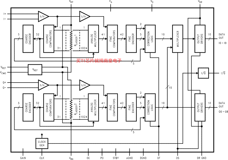
The ADC10D040 is a dual low power, high performance CMOS analog-to-digital converter that digitizes signals to 10 bits resolution at sampling rates up to 45 MSPS while consuming a typical 267 mW from a single 3.3V supply. No missing codes is specified over the full operating temperature range. The unique two stage architecture achieves 9.4 Effective Bits over the entire Nyquist band at 40 MHz sample rate. An output formatting choice of offset binary or 2's complement coding and a choice of two gain settings eases the interface to many systems. Also allowing great flexibility of use is a selectable 10-bit multiplexed or 20-bit parallel output mode. An offset correction feature minimizes the offset error.
To ease interfacing to most low voltage systems, the digital output power pins of the ADC10D040 can be tied to a separate supply voltage of 1.5V to 3.6V, making the outputs compatible with other low voltage systems. When not converting, power consumption can be reduced by pulling the PD (Power Down) pin high, placing the converter into a low power state where it typically consumes less than 1 mW and from which recovery is less than 1 ms. Bringing the STBY (Standby) pin high places the converter into a standby mode where power consumption is about 30 mW and from which recovery is 800 ns.
The ADC10D040's speed, resolution and single supply operation make it well suited for a variety of applications, including high speed portable applications.
Operating over the industrial (−40° ≤ TA ≤ +85°C) temperature range, the ADC10D040 is available in a 48-pin TQFP. An evaluation board is available to ease the design effort.
- Internal Sample-and-Hold
- Internal Reference Capability
- Dual Gain Settings
- Offset Correction
- Selectable Offset Binary or 2's Complement Output
- Multiplexed or Parallel Output Bus
- Single +3.0V to 3.6V Operation
- Power Down and Standby Modes
- 3V TTL Logic Input/Output Compatible
- Resolution: 10 Bits
- Conversion Rate: 40 MSPS
- ENOB: 9.4 Bits (typ)
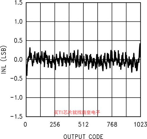
- DNL: 0.35 LSB (typ)
- Conversion Latency Parallel Outputs: 2.5 Clock Cycles
- Multiplexed Outputs, I Data Bus: 2.5 Clock Cycles
- Multiplexed Outputs, Q Data Bus: 3 Clock Cycles
- PSRR: 90 dB
- Power Consumption―Normal Operation: 267 mW (typ)
- Power Down Mode: < 1 mW (typ)
- Fast Recovery Standby Mode: 30 mW (typ)
All trademarks are the property of their respective owners.
- Sample rate (Max) (MSPS)
- 40
- Resolution (Bits)
- 10
- Number of input channels
- 2
- Interface type
- Parallel CMOS, TTL
- Analog input BW (MHz)
- 140
- Features
- Low Power
- Rating
- Catalog
- Input range (Vp-p)
- 1.4
- Power consumption (Typ) (mW)
- 267
- Architecture
- Two-Step
- SNR (dB)
- 60
- ENOB (Bits)
- 9.5
- SFDR (dB)
- 72
- Operating temperature range (C)
- -40 to 85
- Input buffer
- No
ADC10D040的完整型号有:ADC10D040CIVS/NOPB,以下是这些产品的关键参数及官网采购报价:
ADC10D040CIVS/NOPB,工作温度:-40 to 85,封装:TQFP (PFB)-48,包装数量MPQ:250个,MSL 等级/回流焊峰值温度:Level-3-260C-168 HR,引脚镀层/焊球材料:SN,TI官网ADC10D040CIVS/NOPB的批量USD价格:6.486(1000+)

ADC10D040 IBIS Model
PSpice for TI 可提供帮助评估模拟电路功能的设计和仿真环境。此功能齐全的设计和仿真套件使用 Cadence 的模拟分析引擎。PSpice for TI 可免费使用,包括业内超大的模型库之一,涵盖我们的模拟和电源产品系列以及精选的模拟行为模型。借助?PSpice for TI 的设计和仿真环境及其内置的模型库,您可对复杂的混合信号设计进行仿真。创建完整的终端设备设计和原型解决方案,然后再进行布局和制造,可缩短产品上市时间并降低开发成本。
在?PSpice for TI 设计和仿真工具中,您可以搜索 TI (...)