- 制造厂商:TI
- 产品类别:数据转换器
- 技术类目:模数转换器 (ADC) - 高速模数转换器 (>10MSPS)
- 功能描述:耐辐射加固保障 (RHA)、100krad、陶瓷、10 位、双通道 1GSPS 或单通道 2GSPS ADC
- 点击这里打开及下载ADC10D1000QML-SP的技术文档资料
- TI代理渠道,提供当日发货、严格的质量标准,满足您的目标价格

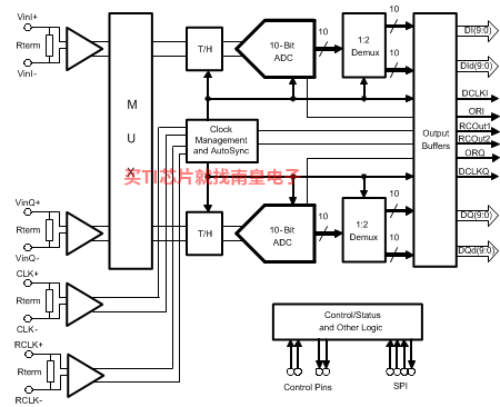
The ADC10D1000 is the latest advance in TI's Ultra-High-Speed ADC family of products. This low-power, high-performance CMOS analog-to-digital converter digitizes signals at 10-bit resolution at sampling rates of up to 1.0 GSPS in dual channel mode or 2.0 GSPS in single channel mode. The ADC10D1000 achieves excellent accuracy and dynamic performance while consuming a typical 2.9 W of power. This space grade, Radiation Tolerant part is rad hard to a single event latch up level of greater than 120MeV and a total dose (TID) of 100 krad(Si). The product is packaged in a hermatic 376 column thermally enhanced CPGA package rated over the temperature range of -55°C to +125°C.
The ADC10D1000 builds upon the features, architecture and functionality of the 8-bit GHz family of ADCs. New features include an auto-sync feature for multi-chip synchronization, independent programmable15-bit gain and 12-bit offset adjustment per channel, LC tank filter on the clock input, and the option of two's complement format for the digital output data. The unique folding and interpolating architecture, the fully differential comparator design, the innovative design of the internal track-and-hold amplifier and the self-calibration scheme enable a very flat response of all dynamic parameters beyond Nyquist, producing a high 8.9 Effective Number of Bits (ENOB) with a 498 MHz input signal and a 1.0 GHz sample rate while providing a 10−18 Code Error Rate (C.E.R.) Consuming a typical 2.9 W in Non-Demultiplex Mode at 1.0 GSPS from a single 1.9-V supply, this device is ensured to have no missing codes over the full operating temperature range.
Each channel has its own independent DDR Data Clock, DCLKI and DCLKQ, which are in phase when both channels are powered up, so that only one Data Clock could be used to capture all data, which is sent out at the same rate as the input sample clock. If the 1:2 Demultiplexed Mode is selected, a second 10-bit LVDS bus becomes active for each channel, such that the output data rate is sent out two times slower, but two times wider to relax data-capture timing margin. The two channels (I and Q) can also be interleaved (DES Mode) and used as a single 2.0 GSPS ADC to sample on the Q input. The output formatting is offset binary or two's complement and the Low Voltage Differential Signaling (LVDS) digital outputs are compatible with IEEE 1596.3-1996, with the exception of an adjustable common mode voltage between 0.8 V and 1.2 V.
- Total Ionizing Dose 100 krad(Si)
- Single Event Latch-Up 120 Mev-cm2/mg
- Excellent Accuracy and Dynamic Performance
- Low Power Consumption
- R/W SPI Interface for Extended Control Mode
- Internally Terminated, Buffered, Differential Analog Inputs
- Ability to Interleave the 2 Channels to Operate 1 Channel at Twice the Conversion Rate
- Test Patterns at Output for System Debug
- Programmable 15-Bit Gain and 12-Bit Plus Sign Offset Adjustments
- Option of 1:2 Demuxed or 1:1 Non-demuxed LVDS Outputs
- Auto-sync Feature for Multi-chip Systems
- Single 1.9 ±0.1-V Power Supply
- 376 Ceramic Pin Grid Array Package (28.2 mm x 28.2 mm x 3.1 mm with 1.27 mm ball-pitch)
- Sample rate (Max) (MSPS)
- 1000, 2000
- Resolution (Bits)
- 10
- Number of input channels
- 2, 1
- Interface type
- Parallel LVDS
- Analog input BW (MHz)
- 2800
- Features
- Ultra High Speed
- Rating
- Space
- Input range (Vp-p)
- 0.8
- Power consumption (Typ) (mW)
- 2770
- Architecture
- Folding Interpolating
- SNR (dB)
- 56.8
- ENOB (Bits)
- 9
- SFDR (dB)
- 67.6
- Operating temperature range (C)
- -55 to 125, 25 to 25
- Input buffer
- Yes
ADC10D1000QML-SP的完整型号有:ADC10D1000CCMLS、ADC10D1000CCMPR,以下是这些产品的关键参数及官网采购报价:
ADC10D1000CCMLS,工作温度:-55 to 125,封装:CCGA (NAA)-376,包装数量MPQ:1个,MSL 等级/回流焊峰值温度:Call TI,引脚镀层/焊球材料:Call TI,TI官网ADC10D1000CCMLS的批量USD价格:23284.8(1000+)
ADC10D1000CCMPR,工作温度:25 to 25,封装:CCGA (NAA)-376,包装数量MPQ:1个,MSL 等级/回流焊峰值温度:Call TI,引脚镀层/焊球材料:Call TI,TI官网ADC10D1000CCMPR的批量USD价格:5758.5(1000+)

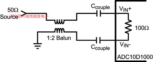
ADC-LD-BB ― ADC 低失真不平衡变压器板
One ADC-LD-BBboard is included in the hardware kit with the GSPS analog-to-digital converter (ADC) reference boards. Since the analog inputs to the ADC1xDxx00RB are differential and most signal sources are single ended, these balun boards are generally used to achieve (...)
ADC-WB-BB ― ADC 宽带不平衡变压器板
OneADC-WB-BB board is included in the hardware kit with the GSPS analog-to-digital converter (ADC) reference boards. Since the analog inputs to the ADC1xDxx00RB are differential and most signal sources are single ended, these balun boards are generally used to achieve (...)
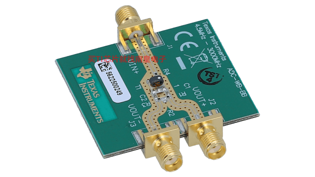
ADC10D1000CVAL ― 10 位双路 1.0 GSPS/单路 2.0 GSPS 信号采集评估板
The ADC10D1000CVAL Evaluation Board populated with a ceramic sample is designed to allow quick evaluation and design development of TI's ADC10D1000CCMLS ultra high speed 10-bit Analog-to-Digital Converter. This evaluation board is designed to function with Agilent's 16702B Logic Analysis System for (...)
ADC10D1000QML IBIS Model
PSpice for TI 可提供帮助评估模拟电路功能的设计和仿真环境。此功能齐全的设计和仿真套件使用 Cadence 的模拟分析引擎。PSpice for TI 可免费使用,包括业内超大的模型库之一,涵盖我们的模拟和电源产品系列以及精选的模拟行为模型。借助?PSpice for TI 的设计和仿真环境及其内置的模型库,您可对复杂的混合信号设计进行仿真。创建完整的终端设备设计和原型解决方案,然后再进行布局和制造,可缩短产品上市时间并降低开发成本。
在?PSpice for TI 设计和仿真工具中,您可以搜索 TI (...)