- 制造厂商:TI
- 产品类别:数据转换器
- 技术类目:模数转换器 (ADC) - 高速模数转换器 (>10MSPS)
- 功能描述:双通道、11 位、105MSPS 模数转换器 (ADC)
- 点击这里打开及下载ADC11DS105的技术文档资料
- TI代理渠道,提供当日发货、严格的质量标准,满足您的目标价格

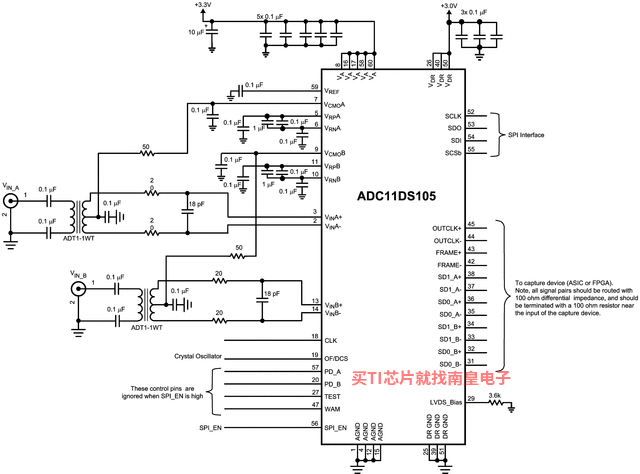
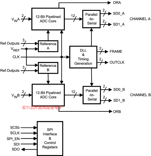
The ADC11DS105is a high-performance CMOS analog-to-digital converters capable of converting two analog input signals into 11-bit digital words at rates up to 105 Mega Samples Per Second (MSPS). The digital outputs are serialized and provided on differential LVDS signal pairs. These converters use a differential, pipelined architecture with digital error correction and an on-chip sample-and-hold circuit to minimize power consumption and the external component count, while providing excellent dynamic performance. The ADC11DS105 may be operated from a single +3.0 or +3.3V power supply. A power-down feature reduces the power consumption to very low levels while still allowing fast wake-up time to full operation. The differential inputs accept a 2V full scale differential input swing. A stable 1.2V internal voltage reference is provided, or the ADC11DS105 can be operated with an external 1.2V reference. The selectable duty cycle stabilizer maintains performance over a wide range of clock duty cycles. A serial interface allows access to the internal registers for full control of the ADC11DS105's functionality. The ADC11DS105 is available in a 60-lead WQFN package and operates over the industrial temperature range of −40°C to +85°C.
- Clock Duty Cycle Stabilizer
- Single +3.0 or +3.3V Supply Operation
- Serial LVDS Outputs
- Serial Control Interface
- Overrange Outputs
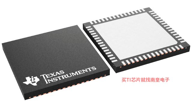
- 60-Pin WQFN Package, (9x9x0.8mm, 0.5mm Pin-Pitch)
- Resolution 11 Bits
- Conversion Rate 105 MSPS
- SNR (fIN = 240 MHz) 66 dBFS (typ)
- SFDR (fIN = 240 MHz) 82 dBFS (typ)
- Full Power Bandwidth 1 GHz (typ)
- Power Consumption 1 W (typ)
All trademarks are the property of their respective owners.
- Sample rate (Max) (MSPS)
- 105
- Resolution (Bits)
- 11
- Number of input channels
- 2
- Interface type
- Serial LVDS
- Analog input BW (MHz)
- 1000
- Features
- Low Power
- Rating
- Catalog
- Input range (Vp-p)
- 2
- Power consumption (Typ) (mW)
- 1000
- Architecture
- Pipeline
- SNR (dB)
- 67
- ENOB (Bits)
- 10.9
- SFDR (dB)
- 88
- Operating temperature range (C)
- -40 to 85
- Input buffer
- No
ADC11DS105的完整型号有:ADC11DS105CISQE/NOPB,以下是这些产品的关键参数及官网采购报价:
ADC11DS105CISQE/NOPB,工作温度:-40 to 85,封装:WQFN (NKA)-60,包装数量MPQ:250个,MSL 等级/回流焊峰值温度:Level-3-260C-168 HR,引脚镀层/焊球材料:SN,TI官网ADC11DS105CISQE/NOPB的批量USD价格:40.075(1000+)

PSPICE-FOR-TI ― 适用于 TI 设计和模拟工具的 PSpice
PSpice for TI 可提供帮助评估模拟电路功能的设计和仿真环境。此功能齐全的设计和仿真套件使用 Cadence 的模拟分析引擎。PSpice for TI 可免费使用,包括业内超大的模型库之一,涵盖我们的模拟和电源产品系列以及精选的模拟行为模型。借助?PSpice for TI 的设计和仿真环境及其内置的模型库,您可对复杂的混合信号设计进行仿真。创建完整的终端设备设计和原型解决方案,然后再进行布局和制造,可缩短产品上市时间并降低开发成本。
在?PSpice for TI 设计和仿真工具中,您可以搜索 TI (...)
