- 制造厂商:TI
- 产品类别:数据转换器
- 技术类目:模数转换器 (ADC) - 高速模数转换器 (>10MSPS)
- 功能描述:双通道、12 位、40MSPS 模数转换器 (ADC)
- 点击这里打开及下载ADC12DL040的技术文档资料
- TI代理渠道,提供当日发货、严格的质量标准,满足您的目标价格

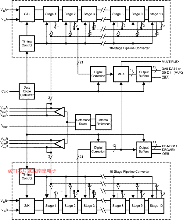
The ADC12DL040 is a dual, low power monolithic CMOS analog-to-digital converter capable of converting analog input signals into 12-bit digital words at 40 Megasamples per second (MSPS). This converter uses a differential, pipeline architecture with digital error correction and an on-chip sample-and-hold circuit to minimize power consumption while providing excellent dynamic performance and a 250 MHz Full Power Bandwidth. Operating on a single +3.0V power supply, the ADC12DL040 achieves 11.1 effective bits at nyquist and consumes just 210 mW at 40 MSPS, including the reference current. The Power Down feature reduces power consumption to 36 mW.
The differential inputs provide a full scale differential input swing equal to 2 times VREF with the possibility of a single-ended input. Full use of the differential input is recommended for optimum performance. The digital outputs from the two ADC's are available on a single multiplexed 12-bit bus or on separate buses. Duty cycle stabilization and output data format are selectable using a quad state function pin. The output data can be set for offset binary or two's complement.
To ease interfacing to lower voltage systems, the digital output driver power pins of the ADC12DL040 can be connected to a separate supply voltage in the range of 2.4V to the analog supply voltage.
This device is available in the 64-lead TQFP package and will operate over the industrial temperature range of −40°C to +85°C. An evaluation board is available to ease the evaluation process.
- Single +3.0V Supply Operation
- Internal Sample-and-Hold
- Internal Reference
- Outputs 2.4V to 3.6V Compatible
- Power Down Mode
- Duty Cycle Stabilizer
- Multiplexed Output Mode
- Resolution 12 Bits
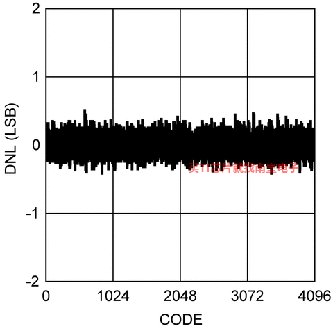
- DNL ±0.3 LSB (typ)
- SNR (fIN = 10 MHz) 69 dB (typ)
- SFDR (fIN = 10 MHz) 85 dB (typ)
- Data Latency 7 Clock Cycles
- Power Consumption
- Operating 210 mW (typ)
- Power Down Mode 36 mW (typ)
All trademarks are the property of their respective owners. TRI-STATE is a trademark of Texas Instruments.
- Sample rate (Max) (MSPS)
- 40
- Resolution (Bits)
- 12
- Number of input channels
- 2
- Interface type
- Parallel CMOS, TTL
- Analog input BW (MHz)
- 250
- Features
- Low Power
- Rating
- Catalog
- Input range (Vp-p)
- 2
- Power consumption (Typ) (mW)
- 210
- Architecture
- Pipeline
- SNR (dB)
- 69
- ENOB (Bits)
- 11.1
- SFDR (dB)
- 86
- Operating temperature range (C)
- -40 to 85
- Input buffer
- No
ADC12DL040的完整型号有:ADC12DL040CIVS/NOPB、ADC12DL040CIVSX/NOPB,以下是这些产品的关键参数及官网采购报价:
ADC12DL040CIVS/NOPB,工作温度:-40 to 85,封装:TQFP (PAG)-64,包装数量MPQ:160个,MSL 等级/回流焊峰值温度:Level-3-260C-168 HR,引脚镀层/焊球材料:SN,TI官网ADC12DL040CIVS/NOPB的批量USD价格:11.616(1000+)
ADC12DL040CIVSX/NOPB,工作温度:-40 to 85,封装:TQFP (PAG)-64,包装数量MPQ:1000个,MSL 等级/回流焊峰值温度:Level-3-260C-168 HR,引脚镀层/焊球材料:SN,TI官网ADC12DL040CIVSX/NOPB的批量USD价格:9.68(1000+)

ADC12DL040 IBIS Model
PSpice for TI 可提供帮助评估模拟电路功能的设计和仿真环境。此功能齐全的设计和仿真套件使用 Cadence 的模拟分析引擎。PSpice for TI 可免费使用,包括业内超大的模型库之一,涵盖我们的模拟和电源产品系列以及精选的模拟行为模型。借助?PSpice for TI 的设计和仿真环境及其内置的模型库,您可对复杂的混合信号设计进行仿真。创建完整的终端设备设计和原型解决方案,然后再进行布局和制造,可缩短产品上市时间并降低开发成本。
在?PSpice for TI 设计和仿真工具中,您可以搜索 TI (...)