- 制造厂商:TI
- 产品类别:数据转换器
- 技术类目:模数转换器 (ADC) - 高速模数转换器 (>10MSPS)
- 功能描述:16 位、130MSPS 模数转换器 (ADC)
- 点击这里打开及下载ADC16V130的技术文档资料
- TI代理渠道,提供当日发货、严格的质量标准,满足您的目标价格

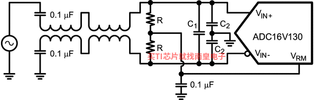
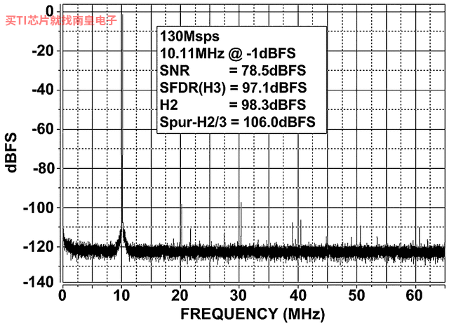
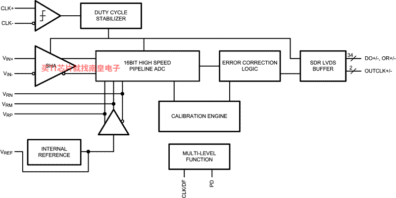
The ADC16V130 is a monolithic high performance CMOS analog-to-digital converter capable of converting analog input signals into 16-bit digital words at rates up to 130 Mega Samples Per Second (MSPS). This converter uses a differential, pipelined architecture with digital error correction and an on-chip sample-and-hold circuit to minimize power consumption and external component count while providing excellent dynamic performance. Automatic power-up calibration enables excellent dynamic performance and reduces part-to-part variation, and the ADC16V130 could be re-calibrated at any time by asserting and then de-asserting power-down. An integrated low noise and stable voltage reference and differential reference buffer amplifier easies board level design. On-chip duty cycle stabilizer with low additive jitter allows wide duty cycle range of input clock without compromising its dynamic performance. A unique sample-and-hold stage yields a full-power bandwidth of 1.4 GHz. The digital data is provided via full data rate LVDS outputs – making possible the 64-pin, 9mm x 9mm WQFN package. The ADC16V130 operates on dual power supplies +1.8V and +3.0V with a power-down feature to reduce the power consumption to very low levels while allowing fast recovery to full operation.
- Dual Supplies: 1.8V and 3.0V Operation
- On Chip Automatic Calibration During Power-Up
- Low Power Consumption
- Multi-Level Multi-Function Pins for CLK/DF and PD
- Power-Down and Sleep Modes
- On Chip Precision Reference and Sample-and-Hold Circuit
- On Chip Low Jitter Duty-Cycle Stabilizer
- Offset Binary or 2's Complement Data Format
- Full Data Rate LVDS Output Port
- 64-pin WQFN Package (9x9x0.8, 0.5mm Pin-Pitch)
- High IF Sampling Receivers
- Multi-carrier Base Station Receivers
- GSM/EDGE, CDMA2000, UMTS, LTE, and WiMax
- Test and Measurement Equipment
- Communications Instrumentation
- Data Acquisition
- Portable Instrumentation
All trademarks are the property of their respective owners.
- Sample rate (Max) (MSPS)
- 130
- Resolution (Bits)
- 16
- Number of input channels
- 1
- Interface type
- Parallel LVDS
- Analog input BW (MHz)
- 1400
- Features
- High Performance
- Rating
- Catalog
- Input range (Vp-p)
- 2.4
- Power consumption (Typ) (mW)
- 755
- Architecture
- Pipeline
- SNR (dB)
- 78.5
- ENOB (Bits)
- 12.7
- SFDR (dB)
- 95.5
- Operating temperature range (C)
- -40 to 85
- Input buffer
- No
ADC16V130的完整型号有:ADC16V130CISQ/NOPB、ADC16V130CISQE/NOPB、ADC16V130CISQX/NOPB,以下是这些产品的关键参数及官网采购报价:
ADC16V130CISQ/NOPB,工作温度:-40 to 85,封装:WQFN (NKD)-64,包装数量MPQ:250个,MSL 等级/回流焊峰值温度:Level-3-260C-168 HR,引脚镀层/焊球材料:SN,TI官网ADC16V130CISQ/NOPB的批量USD价格:65.501(1000+)
ADC16V130CISQE/NOPB,工作温度:-40 to 85,封装:WQFN (NKD)-64,包装数量MPQ:250个,MSL 等级/回流焊峰值温度:Level-3-260C-168 HR,引脚镀层/焊球材料:SN,TI官网ADC16V130CISQE/NOPB的批量USD价格:65.501(1000+)
ADC16V130CISQX/NOPB,工作温度:-40 to 85,封装:WQFN (NKD)-64,包装数量MPQ:2000个,MSL 等级/回流焊峰值温度:Level-3-260C-168 HR,引脚镀层/焊球材料:SN,TI官网ADC16V130CISQX/NOPB的批量USD价格:63.501(1000+)

WAVEVISION5 ― Data Acquisition and Analysis Software
WaveVision 5 software is part of the WaveVision evaluation system that also includes WaveVision 5 Data Capture Board. The WaveVision 5 system is an easy-to-use data acquisition and analysis tool, designed to help users evaluate Texas Instruments' Signal Path solutions.While WaveVision 5 software (...)
PSPICE-FOR-TI ― 适用于 TI 设计和模拟工具的 PSpice
PSpice for TI 可提供帮助评估模拟电路功能的设计和仿真环境。此功能齐全的设计和仿真套件使用 Cadence 的模拟分析引擎。PSpice for TI 可免费使用,包括业内超大的模型库之一,涵盖我们的模拟和电源产品系列以及精选的模拟行为模型。借助?PSpice for TI 的设计和仿真环境及其内置的模型库,您可对复杂的混合信号设计进行仿真。创建完整的终端设备设计和原型解决方案,然后再进行布局和制造,可缩短产品上市时间并降低开发成本。
在?PSpice for TI 设计和仿真工具中,您可以搜索 TI (...)