- ���쳧�̣�TI
- ��Ʒ�������ת����
- ������Ŀ��ģ��ת���� (ADC) - ����ģ��ת���� (>10MSPS)
- ����������QMLV��150krad���մɡ�14 λ����ͨ�� 125MSPS ADC
- ������������ADS5424-SP�ļ����ĵ�����
- TI�����������ṩ���շ������ϸ������������������Ŀ��۸�

The ADS5424 is a 14-bit, 105-MSPS analog-to-digital converter (ADC) that operates from a 5-V supply, while providing 3.3-V CMOS compatible digital outputs. The ADS5424 input buffer isolates the internal switching of the on-chip track and hold (T&H) from disturbing the signal source. An internal reference generator is also provided to further simplify the system design. The ADS5424 has outstanding low noise and linearity, over input frequency. With only a 2.2-VPP input range, ADS5424 simplifies the design of multicarrier applications, where the carriers are selected on the digital domain.
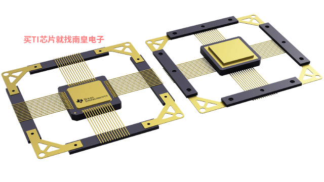
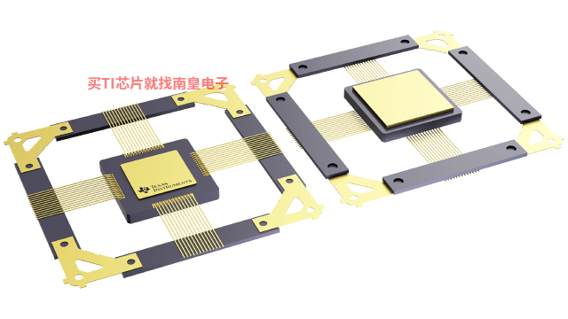
The ADS5424 is available in a 52-pin ceramic nonconductive tie-bar package (HFG). The ADS5424 is built on state of the art Texas Instruments complementary bipolar process (BiCom3) and is specified over full military temperature range (–55°C to 125°C Tcase)
This CQFP package has built-in vias that electrically and thermally connect the bottom of the die to a pad on the bottom of the package. To efficiently remove heat and provide a low-impedance ground path, a thermal land is required on the surface of the PCB directly underneath the body of the package. During normal surface mount flow solder operations, the heat pad on the underside of the package is soldered to this thermal land creating an efficient thermal path. Normally, the PCB thermal land has a number of thermal vias within it that provide a thermal path to internal copper areas (or to the opposite side of the PCB) that provide for more efficient heat removal. TI typically recommends a 16-mm2 board-mount thermal pad. This allows maximum area for thermal dissipation, while keeping leads away from the pad area to prevent solder bridging. A sufficient quantity of thermal/electrical vias must be included to keep the device within recommended operating conditions. This pad must be electrically at ground potential.
- 14-Bit Resolution
- 105-MSPS Maximum Sample Rate
- SNR = 70 dBc at 105 MSPS and 50 MHz IF
- SFDR = 78 dBc at 105 MSPS and 50 MHz IF
- 2.2-VPP Differential Input Range
- 5-V Supply Operation
- 3.3-V CMOS Compatible Outputs
- 2.3-W Total Power Dissipation
- 2s Complement Output Format
- On-Chip Input Analog Buffer, Track and Hold, and Reference Circuit
- 52-Pin Ceramic Nonconductive Tie-Bar Package (HFG)
- Military Temperature Range ( �C55��C to 125��C Tcase)
- QML-V Qualified, SMD 5962-07206
- Engineering Evaluation (/EM) Samples are Available(1)
- APPLICATIONS
- Single and Multichannel Digital Receivers
- Base Station Infrastructure
- Instrumentation
- Video and Imaging
- Clocking: CDC7005
- Amplifiers: OPA695, THS4509
(1) These units are intended for engineering evaluation only. They are processed to a non-compliant flow (e.g. No Burn-In, etc.) and are tested to a temperature rating of 25��C only. These units are not suitable for qualification, production, radiation testing or flight use. Parts are not warranted for performance over the full MIL specified temperature range of �C55��C to 125��C or operating life.
- Sample rate (Max) (MSPS)
- 105
- Resolution (Bits)
- 14
- Number of input channels
- 1
- Interface type
- Parallel CMOS
- Analog input BW (MHz)
- 570
- Features
- High Performance
- Rating
- Space
- Input range (Vp-p)
- 2.2
- Power consumption (Typ) (mW)
- 1900
- Architecture
- Pipeline
- SNR (dB)
- 72.4
- ENOB (Bits)
- 11.7
- SFDR (dB)
- 82.6
- Operating temperature range (C)
- -55 to 125, 25 to 25
- Input buffer
- No
ADS5424-SP�������ͺ��У�5962-0720601VXC��ADS5424HFG/EM����������Щ��Ʒ�Ĺؼ������������ɹ����ۣ�
5962-0720601VXC�������¶ȣ�-55 to 125����װ��CFP (HFG)-52����װ����MPQ��1����MSL �ȼ�/��������ֵ�¶ȣ�N/A for Pkg Type�����ŶƲ�/������ϣ�Call TI��TI����5962-0720601VXC������USD�۸�5636.789��1000+��
ADS5424HFG/EM�������¶ȣ�25 to 25����װ��CFP (HFG)-52����װ����MPQ��1����MSL �ȼ�/��������ֵ�¶ȣ�N/A for Pkg Type�����ŶƲ�/������ϣ�Call TI��TI����ADS5424HFG/EM������USD�۸�1573.95��1000+��

ADS5424-SP IBIS MDOEL
PSpice for TI ���ṩ��������ģ���·���ܵ���ƺͷ��滷�����˹�����ȫ����ƺͷ�����ʹ�� Cadence ��ģ��������档PSpice for TI �����ʹ�ã�����ҵ�ڳ����ģ�Ϳ�֮һ���������ǵ�ģ��͵�Դ��Ʒϵ���Լ���ѡ��ģ����Ϊģ�͡�����?PSpice for TI ����ƺͷ��滷���������õ�ģ�Ϳ⣬���ɶԸ��ӵĻ���ź���ƽ��з��档�����������ն��豸��ƺ�ԭ�ͽ��������Ȼ���ٽ��в��ֺ����죬�����̲�Ʒ����ʱ�䲢���Ϳ����ɱ���
��?PSpice for TI ��ƺͷ��湤���У����������� TI (...)


