- 制造厂商:TI
- 产品类别:数据转换器
- 技术类目:模数转换器 (ADC) - 高速模数转换器 (>10MSPS)
- 功能描述:双通道、11 位、200MSPS 模数转换器 (ADC)
- 点击这里打开及下载ADS58C28的技术文档资料
- TI代理渠道,提供当日发货、严格的质量标准,满足您的目标价格

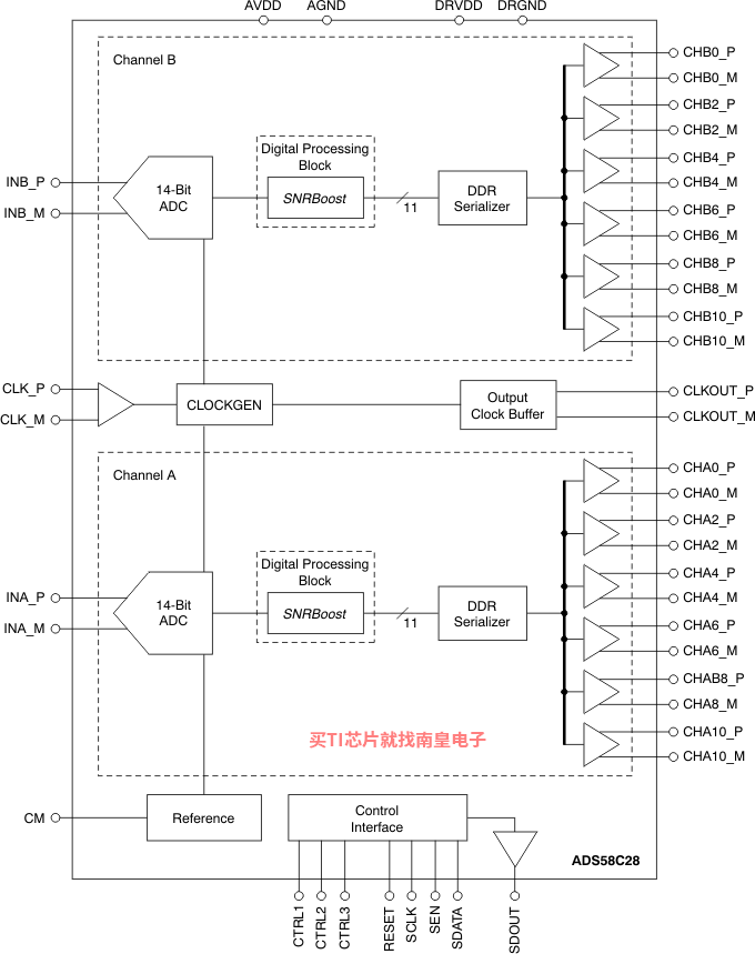
The ADS58C28 is a dual-channel, 11-bit analog-to-digital converter (ADC) with sampling rates up to 200MSPS. The device uses innovative design techniques to achieve high dynamic performance, while consuming extremely low power at 1.8V supply. This architecture makes it well-suited for multi-carrier, wide bandwidth communications applications.
The ADS58C28 uses third-generation SNRBoost3G technology to overcome SNR limitation as a result of quantization noise (for bandwidths less than Nyquist, fS/2). Enhancements in the SNRBoost3G technology allow support for SNR improvements over wide bandwidths (up to 60MHz). In addition, separate SNRBoost3G coefficients can also be programmed for each channel.
The device has a digital gain function that can be used to improve SFDR performance at lower full-scale input ranges. It includes a dc offset correction loop that can be used to cancel the ADC offset. The digital outputs of all channels are output as double data rate (DDR) low-voltage differential signaling (LVDS) together with an LVDS clock output. The low data rate of this interface (400MBPS at 200MSPS sample rate) makes it possible to use low-cost field-programmable gate array (FPGA)-based receivers. The strength of the LVDS output buffers can be increased to support 50Ω differential termination. This increase allows the output clock signal to be connected to two separate receiver chips with an effective 50Ω termination (such as the two clock ports of the GC5330). The same digital output pins can also be configured as a parallel 1.8V CMOS interface.
The device includes internal references while the traditional reference pins and associated decoupling capacitors have been eliminated. The ADS58C28 is specified over the industrial temperature range (–40°C to +85°C).
- Maximum Sample Rate: 200MSPS
- High Dynamic Performance:
- 83dBc SFDR at 140MHz
- 72.5dBFS SNR with 60MHz BW Using SNRBoost3G Technology
- SNRBoost3G Highlights:
- Supports Wide Bandwidth (up to 60MHz)
- Programmable Bandwidths: 20MHz, 30MHz, and 40MHz
- Flat Noise Floor within the Band
- Independent SNRBoost3G Coefficients for Both Channels
- Output Interface:
- Double Data Rate (DDR) LVDS with Programmable Swing and Strength:
- Standard Swing: 350mV
- Low Swing: 200mV
- Default Strength: 100Ω termination
- 2× Strength: 50Ω termination
- Compatible with GC6016
- 1.8V Parallel CMOS Interface Also Supported
- Double Data Rate (DDR) LVDS with Programmable Swing and Strength:
- Ultralow Power with Single 1.8V Supply:
- 470mW Total Power
- 710mW Total Power (200MSPS) with SNRBoost3G on Both Channels
- Programmable Gain up to 6dB for SNR/SFDR Trade-off
- DC Offset Correction
- Supports Low Input Clock Amplitude
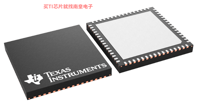
- Package: QFN-64 (9mm × 9mm)
PowerPAD is a trademark of Texas Instruments Incorporated. All other trademarks are the property of their respective owners
- Sample rate (Max) (MSPS)
- 200
- Resolution (Bits)
- 11
- Number of input channels
- 2
- Interface type
- Parallel CMOS, Parallel LVDS
- Analog input BW (MHz)
- 600
- Features
- High Performance
- Rating
- Catalog
- Input range (Vp-p)
- 2
- Power consumption (Typ) (mW)
- 505
- Architecture
- Pipeline
- SNR (dB)
- 66.8
- ENOB (Bits)
- 10.7
- SFDR (dB)
- 84
- Operating temperature range (C)
- -40 to 85
- Input buffer
- No
ADS58C28的完整型号有:ADS58C28IRGCR、ADS58C28IRGCT,以下是这些产品的关键参数及官网采购报价:
ADS58C28IRGCR,工作温度:-40 to 85,封装:VQFN (RGC)-64,包装数量MPQ:2000个,MSL 等级/回流焊峰值温度:Level-3-260C-168 HR,引脚镀层/焊球材料:NIPDAU,TI官网ADS58C28IRGCR的批量USD价格:61.904(1000+)
ADS58C28IRGCT,工作温度:-40 to 85,封装:VQFN (RGC)-64,包装数量MPQ:250个,MSL 等级/回流焊峰值温度:Level-3-260C-168 HR,引脚镀层/焊球材料:NIPDAU,TI官网ADS58C28IRGCT的批量USD价格:63.904(1000+)

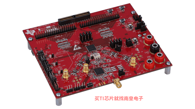
ADS58C28EVM ― ADS58C28 评估模块
ADS58C28EVM 是能够让设计者评估德州仪器 (TI) ADS58C28 器件(采用 TI SNRBoost 技术的 11 位 200MSPS 双通道模数转换器)的电路板。ADC EVM 采用与 TI 的 TSW1200 数据采集卡兼容的 DDR LVDS 数据输出,以便快速评估。EVM 提供了可在各种时钟、输入和电源条件下测试 ADS58C28 的灵活环境。
该评估模块针对转换器的四个输入都设计有背对背宽带非平衡转换器。这样就可以将大范围的单端输入信号输入任何 ADC 通道。ADS58C28EVM 还兼容 FMC-ADC-Adapter 和 HSMC-ADC-Bridge (...)
ADS42xxx SPI GUI (Rev. B)
此高速数据转换器专业 GUI 是一款 PC 程序(兼容 Windows XP/7/10),旨在帮助评估大多数 TI 高速数据转换器和模拟前端 (AFE) 平台。DATACONVERTERPRO-SW 支持整个 TSW14xxx 系列的数据采集和模式生成卡,为分析时域和频域中的数据转换器提供了快速强大的解决方案以及单音调、多音调和调制信号支持。此 GUI 还兼容用于快速合成单音调、多音调和调制信号的 TI 模式生成 GUI。用户可以为 DATACONVERTERPRO-SW 提供定制模式,以加载到 TI 数模转换器 (DAC)。支持从模数转换器 (ADC) 采集内导出 CSV (...)
TIGAR Support Files
PSpice for TI 可提供帮助评估模拟电路功能的设计和仿真环境。此功能齐全的设计和仿真套件使用 Cadence 的模拟分析引擎。PSpice for TI 可免费使用,包括业内超大的模型库之一,涵盖我们的模拟和电源产品系列以及精选的模拟行为模型。借助?PSpice for TI 的设计和仿真环境及其内置的模型库,您可对复杂的混合信号设计进行仿真。创建完整的终端设备设计和原型解决方案,然后再进行布局和制造,可缩短产品上市时间并降低开发成本。
在?PSpice for TI 设计和仿真工具中,您可以搜索 TI (...)
JITTER-SNR-CALC ― 用于 ADC 的抖动和 SNR 计算器
JITTER-SNR-CALC 可用于根据输入频率和时钟抖动来计算 ADC 的理论信噪比 (SNR) 性能。