- 制造厂商:TI
- 产品类别:数据转换器
- 技术类目:模数转换器 (ADC) - 高速模数转换器 (>10MSPS)
- 功能描述:14 位、250MSPS 模数转换器 (ADC)
- 点击这里打开及下载ADS61B49的技术文档资料
- TI代理渠道,提供当日发货、严格的质量标准,满足您的目标价格

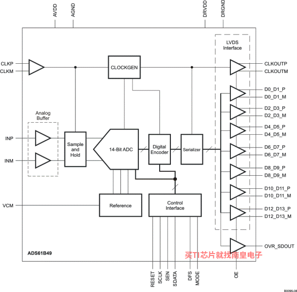
The ADS61B49 (ADS61B29) is a 14-bit (12-bit) A/D converter with a sampling rate up to 250 MSPS. It combines high dynamic performance and low power consumption in a compact 48-QFN package. An integrated analog buffer makes it well-suited for multi-carrier, wide bandwidth communications applications. The buffer maintains constant performance and input impedance across a wide frequency range.
The ADS61B49 (ADS61B29) has fine gain options that can be used to improve SFDR performance at lower full-scale input ranges. It includes a dc offset correction loop that can be used to cancel the ADC offset. Both Double Data Rate (DDR) LVDS and parallel CMOS digital output interfaces are available. At lower sampling rates, the ADC automatically operates at scaled down power with no loss in performance.
It includes internal references while the traditional reference pins and associated decoupling capacitors have been eliminated. The device is specified over the industrial temperature range (-40°C to 85°C).
- Integrated High Impedance Analog Input Buffer
- Maximum Sample Rate: 250 MSPS
- 14-Bit Resolution ― ADS61B49
- 12-Bit Resolution ― ADS61B29
- 790 mW Total Power Dissipation at 250 MSPS
- Double Data Rate (DDR) LVDS and Parallel CMOS Output Options
- Programmable Fine Gain up to 6 dB for SNR/SFDR Trade-Off and 1-Vpp Full-Scale Operation
- DC Offset Correction
- Supports Input Clock Amplitude Down to 400 mVPP Differential
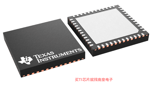
- 48-QFN Package (7mm × 7mm)
- Pin Compatible with ADS6149 Family
- APPLICATIONS
- Multicarrier, Wide Bandwidth Communications
- Wireless Multi-Carrier Communications Infrastructure
- Software Defined Radio
- Power Amplifier Linearization Feedback ADC
- 802.16d/e
- Test and Measurement Instrumentation
- High Definition Video
- Medical Imaging
- Radar Systems
- Sample rate (Max) (MSPS)
- 250
- Resolution (Bits)
- 14
- Number of input channels
- 1
- Interface type
- DDR LVDS, Parallel CMOS
- Analog input BW (MHz)
- 700
- Features
- High Performance
- Rating
- Catalog
- Input range (Vp-p)
- 2
- Power consumption (Typ) (mW)
- 790
- Architecture
- Pipeline
- SNR (dB)
- 72.3
- ENOB (Bits)
- 11.3
- SFDR (dB)
- 92
- Operating temperature range (C)
- -40 to 85
- Input buffer
- Yes
ADS61B49的完整型号有:ADS61B49IRGZR、ADS61B49IRGZT,以下是这些产品的关键参数及官网采购报价:
ADS61B49IRGZR,工作温度:-40 to 85,封装:VQFN (RGZ)-48,包装数量MPQ:2500个,MSL 等级/回流焊峰值温度:Level-3-260C-168 HR,引脚镀层/焊球材料:NIPDAUAG,TI官网ADS61B49IRGZR的批量USD价格:127.778(1000+)
ADS61B49IRGZT,工作温度:-40 to 85,封装:VQFN (RGZ)-48,包装数量MPQ:250个,MSL 等级/回流焊峰值温度:Level-3-260C-168 HR,引脚镀层/焊球材料:NIPDAU,TI官网ADS61B49IRGZT的批量USD价格:129.778(1000+)

ADS6125EVM ― ADS6125 评估模块
The ADS6125EVM is a circuit board that allows designers to evaluate the performance of Texas Instruments‘ ADS6125 device, a low power 12-bit 125MSPS analog to digital converter. The ADC features a configurable parallel DDR LVDS or CMOS outputs. The EVM provides a flexible environment to (...)
HSADC-SPI-UTILITY ― 高速 ADC SPI 编程工具
PSpice for TI 可提供帮助评估模拟电路功能的设计和仿真环境。此功能齐全的设计和仿真套件使用 Cadence 的模拟分析引擎。PSpice for TI 可免费使用,包括业内超大的模型库之一,涵盖我们的模拟和电源产品系列以及精选的模拟行为模型。借助?PSpice for TI 的设计和仿真环境及其内置的模型库,您可对复杂的混合信号设计进行仿真。创建完整的终端设备设计和原型解决方案,然后再进行布局和制造,可缩短产品上市时间并降低开发成本。
在?PSpice for TI 设计和仿真工具中,您可以搜索 TI (...)
JITTER-SNR-CALC ― 用于 ADC 的抖动和 SNR 计算器
JITTER-SNR-CALC 可用于根据输入频率和时钟抖动来计算 ADC 的理论信噪比 (SNR) 性能。


