- ���쳧�̣�TI
- ��Ʒ�������ת����
- ������Ŀ��ģ��ת���� (ADC) - ����ģ��ת���� (<=10MSPS)
- ����������1.2V 8 λ 280KSPS ���� ADC
- ������������ADS7868�ļ����ĵ�����
- TI�����������ṩ���շ������ϸ������������������Ŀ��۸�

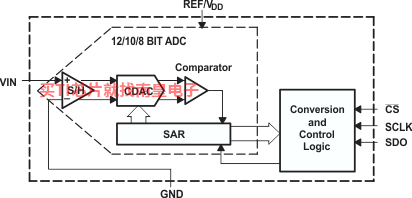
The ADS7866/67/68 are low power, miniature, 12/10/8-bit A/D converters each with a unipolar, single-ended input. These devices can operate from a single 1.6 V to 3.6 V supply with a 200-KSPS throughput for ADS7866. In addition, these devices can maintain at least a 100-KSPS throughput with a supply as low as 1.2 V.
The sampling, conversion, and activation of digital output SDO are initiated on the falling edge of CS\. The serial clock SCLK is used for controlling the conversion rate and shifting data out of the converter. Furthermore, SCLK provides a mechanism to allow digital host processors to synchronize with the con- verter. These converters interface with micro-processors or DSPs through a high-speed SPI compatible serial interface. There are no pipeline delays associated with the device.
The minimum conversion time is determined by the frequency of the serial clock input, SCLK, while the maximum frequency of SCLK is determined by the minimum sampling time required to charge the input capacitance to 12/10/8-bit accuracy for the ADS7866/67/68, respectively. The maximum throughput is determined by how often a conversion is initiated when the minimum sampling time is met and the maximum SCLK frequency is used. Each device automatically powers down after each conversion, which allows each device to save power when the throughput is reduced while using the maximum SCLK frequency.
The converter reference is taken internally from the supply. Hence, the analog input range for these devices is 0 V to VDD.
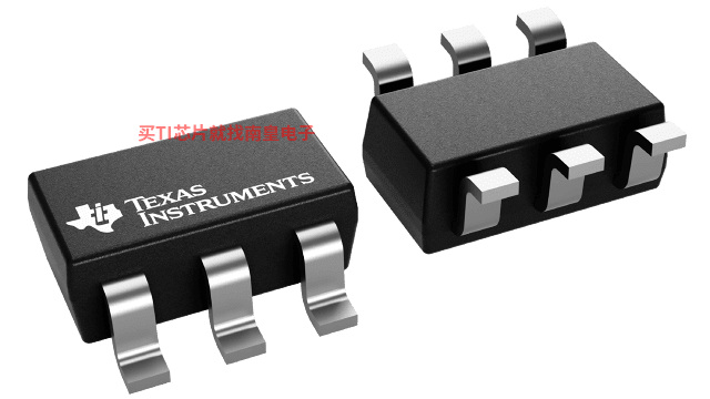
These devices are available in a 6-pin SOT-23 package and are characterized over the industrial –40°C to 85°C temperature range.
- Single 1.2-V to 3.6-V Supply Operation
- High Throughput
- 200/240/280KSPS for 12/10/8-Bit VDD 1.6 V
- 100/120/140KSPS for 12/10/8-Bit VDD 1.2 V
- ��1.5LSB INL, 12-Bit NMC (ADS7866)
- 71 dB SNR, �C83 dB THD at fIN = 30 kHz (ADS7866)
- Synchronized Conversion with SCLK
- SPI Compatible Serial Interface
- No Pipeline Delays
- Low Power
- 1.39 mW Typ at 200 KSPS, VDD = 3.6 V
- 0.39 mW Typ at 200 KSPS, VDD = 1.6 V
- 0.22 mW Typ at 100 KSPS, VDD = 1.2 V
- Auto Power-Down: 8 nA Typ, 300 nA Max
- 0 V to VDD Unipolar Input Range
- 6-Pin SOT-23 Package
- APPLICATIONS
- Battery Powered Systems
- Isolated Data Acquisition
- Medical Instruments
- Portable Communication
- Portable Data Acquisition Systems
- Automatic Test Equipment
- Resolution (Bits)
- 8
- Number of input channels
- 1
- Sample rate (Max) (kSPS)
- 280
- Interface type
- SPI
- Architecture
- SAR
- Input type
- Single-Ended
- Multi-channel configuration
- ��
- Rating
- Catalog
- Reference mode
- Supply
- Input range (Max) (V)
- 3.6
- Input range (Min) (V)
- 0
- Features
- Small Size
- Operating temperature range (C)
- -40 to 85
- Power consumption (Typ) (mW)
- 0.22
- Analog voltage AVDD (Min) (V)
- 1.2
- SNR (dB)
- 49.8
- Analog voltage AVDD (Max) (V)
- 3.6
- INL (Max) (+/-LSB)
- 0.5
- Digital supply (Min) (V)
- 1.2
- Digital supply (Max) (V)
- 3.6
ADS7868�������ͺ��У�ADS7868IDBVR��ADS7868IDBVT����������Щ��Ʒ�Ĺؼ������������ɹ����ۣ�
ADS7868IDBVR�������¶ȣ�-40 to 85����װ��SOT-23 (DBV)-6����װ����MPQ��3000����MSL �ȼ�/��������ֵ�¶ȣ�Level-2-260C-1 YEAR�����ŶƲ�/������ϣ�NIPDAU��TI����ADS7868IDBVR������USD�۸�.66��1000+��
ADS7868IDBVT�������¶ȣ�-40 to 85����װ��SOT-23 (DBV)-6����װ����MPQ��250����MSL �ȼ�/��������ֵ�¶ȣ�Level-2-260C-1 YEAR�����ŶƲ�/������ϣ�NIPDAU��TI����ADS7868IDBVT������USD�۸�.792��1000+��

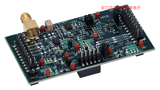
ADS7868EVM �� ADS7868EVM Evaluation Module
The ADS7868EVM is a full-featured reference design, prototype, and software platform for ADS7868 IC. The reference design feature contains essential circuitry to show case the A/D converter. It gives the ability to change the input components to use different input frequencies. As a prototype board (...)
PSPICE-FOR-TI �� ������ TI ��ƺ�ģ��ߵ� PSpice
PSpice for TI ���ṩ��������ģ���·���ܵ���ƺͷ��滷�����˹�����ȫ����ƺͷ�����ʹ�� Cadence ��ģ��������档PSpice for TI �����ʹ�ã�����ҵ�ڳ����ģ�Ϳ�֮һ���������ǵ�ģ��͵�Դ��Ʒϵ���Լ���ѡ��ģ����Ϊģ�͡�����?PSpice for TI ����ƺͷ��滷���������õ�ģ�Ϳ⣬���ɶԸ��ӵĻ���ź���ƽ��з��档�����������ն��豸��ƺ�ԭ�ͽ��������Ȼ���ٽ��в��ֺ����죬�����̲�Ʒ����ʱ�䲢���Ϳ����ɱ���
��?PSpice for TI ��ƺͷ��湤���У����������� TI (...)
TINA-TI �� ���� SPICE ��ģ��������
TINA-TI �ṩ�� SPICE ���еĴ�ͳֱ����˲̬��Ƶ������Լ����ࡣTINA ���й㷺�ĺ������ܣ�����������ϣ���ķ�ʽ���ý���ĸ�ʽ����������������ѡ�����벨�Ρ�̽���·�ڵ��ѹ�Ͳ��Ρ�TINA ��ԭ��ͼ����dz�ֱ�� - �����ġ��������š���TINA-TI ��װ��Ҫ��Լ 500MB��ֱ�Ӱ�װ�������ж��Ҳ�����ס������������϶��ᰮ�����֡�
TINA �ǵ������� (TI) ר�е� DesignSoft ��Ʒ������Ѱ汾���������Ĺ��ܣ�����֧�������� TINA ���ṩ��ijЩ�������ܡ�
�����ȡ���� TINA-TI ģ�͵������б�������ģ�SpiceRack - �����б�
��Ҫ HSpice (...)
ADC-INPUT-CALC �� Analog-to-digital converter (ADC) input driver design tool supporting multiple input types
ADC-INPUT-CALC ��һ�����߹��ߣ���Ϊ���ģ��ת���� (ADC) �����뻺�����ṩ֧�֡����ṩ 24 �ֲ�ͬ�Ļ�������Ŵ����Ļ�������·����Щ��·���������� ADC ���롣�������˺��Dz�ֵ��˺ͱ�ѹ�����������ơ�֧�ֽ�����Ϻ�ֱ���������Լ�����Դ��˫��Դ���ˡ��ṩ����ģʽ����ѧ��ģʽ��ר��ģʽ���ڳ�ѧ��ģʽ�У������Ա�Ȼش�һϵ�����⣬Ȼ��ῴ���������ԭ��ͼ����ijЩ����£����ῴ����������Ŀ�ѡ�汾����ר��ģʽ�£������Ա�ῴ���÷���ͼ��ʽ��ʾ������ 24 (...)ANALOG-ENGINEER-CALC �� ģ���ʦ������
ģ���ʦ������ּ�ڼӿ�ģ���·��ƹ���ʦ����ʹ�õ������ظ��Լ��㡣�û��� PC �Ĺ����ṩͼ�ν��棬������ʾ���ֳ���������б�����ʹ�÷�����������������Ŵ������浽Ϊ�ȶ�ģ��ת���� (ADC) ��������������·ѡ����ʵĵ�·���Ԫ���������˿����������Ĺ���֮�⣬�ü��������ܹ��ܺõ���ģ���ʦ�ڴ��ο����������ĸ������ʹ�á� lock = ��Ҫ�������ɣ�1���ӣ�