- ���쳧�̣�TI
- ��Ʒ�������ת����
- ������Ŀ��������/���������ת���� - ҽ�� AFE
- �������������� 42mW/ͨ�����ʡ�LVDS �ӿں� CW ��Դ��Ƶ���� 32 ͨ�������� AFE
- ������������AFE5832�ļ����ĵ�����
- TI�����������ṩ���շ������ϸ������������������Ŀ��۸�

The AFE5832 device is a highly-integrated, analog front-end solution specifically designed for ultrasound systems where high performance, low power, and small size are required.
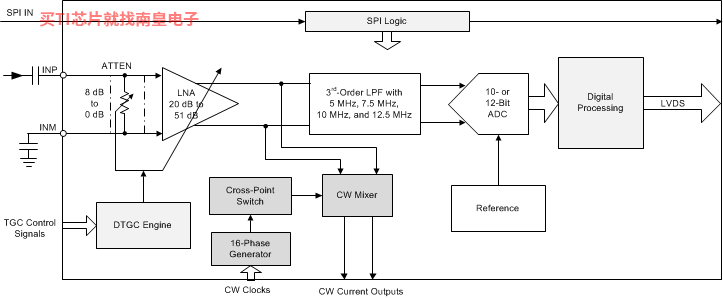
The AFE5832 is an integrated analog front-end (AFE) optimized for medical ultrasound application. The device is realized through a multichip module (MCM) with three dies: two voltage-controlled amplifier (VCA) dies and one analog-to-digital converter (ADC) die. Each VCA die has 16 channels and the ADC die converts all of the 32 channels.
Each channel in the VCA die is configured in either of two modes: time gain compensation (TGC) mode or continuous wave (CW) mode. In TGC mode, each channel includes an input attenuator (ATTEN), a low-noise amplifier (LNA) with variable-gain, and a third-order, low-pass filter (LPF). The attenuator supports an attenuation range of 8 dB to 0 dB, and the LNA supports gain ranges from 20 dB to 51 dB. The LPF cutoff frequency can be configured at 5 MHz, 7.5 MHz, 10 MHz, or 12.5 MHz to support ultrasound applications with different frequencies. In CW mode, each channel includes an LNA with a fixed gain of 18 dB, and a low-power passive mixer with 16 selectable phase delays. Different phase delays can be applied to each analog input signal to perform an on-chip beamforming operation. A harmonic filter in the CW mixer suppresses the third and fifth harmonic to enhance the sensitivity of the CW Doppler measurement.
The ADC die has 16 physical ADCs. Each ADC converts two sets of outputs – one from each VCA die. The ADC is configured to operate with a resolution of 12 bits or 10 bits. The ADC resolution can be traded off with conversion rate, and operates at maximum speeds of 80 MSPS and 100 MSPS at 12-bit and 10-bit resolution, respectively. The ADC is designed to scale its power with sampling rate. The output interface of the ADC comes out through a low-voltage differential signaling (LVDS) which can easily interface with low-cost field-programmable gate arrays (FPGAs).
The AFE5832 also allows various power and noise combinations to be selected for optimizing system performance. Therefore, this device is a suitable ultrasound AFE solution for systems with strict battery-life requirements.
- 32-Channel, AFE for Ultrasound Applications:
- Input Attenuator, LNA, LPF, ADC, and CW Mixer
- Digital Time Gain Compensation (DTGC)
- Total Gain Range: 12 dB to 51 dB
- Linear Input Range: 800 mVPP
- Input Attenuator With DTGC:
- 8-dB to 0-dB Attenuation With 0.125-dB Step
- Supports Matched Impedance for:
- 50-�� to 800-�� Source Impedance
- Low-Noise Amplifier (LNA) With DTGC:
- 20-dB to 51-dB Gain With 0.125-dB Step
- Low Input Current Noise: 1.2 pA/��Hz
- 3rd-Order, Linear-Phase, Low-Pass Filter (LPF):
- 5 MHz, 7.5 MHz, 10 MHz, and 12.5 MHz
- 16 ADCs Converting at 12-Bit, 80 MSPS or 10-bit, 100 MSPS:
- Each ADC Converts Two Sets of Inputs at Half Rate
- 12-Bit ADC: 72-dBFS SNR
- 10-Bit ADC: 61-dBFS SNR
- Optimized for Noise and Power:
- 35 mW/Ch at 2.1 nV/��Hz, 40 MSPS
- 42 mW/Ch at 1.4 nV/��Hz, 40 MSPS
- 52 mW/Ch at 1.3 nV/��Hz, 40 MSPS
- 60 mW/Ch in CW Mode
- Excellent Device-to-Device Gain Matching:
- ��0.5 dB (Typical)
- Low Harmonic Distortion: �C55 dBc
- Fast and Consistent Overload Recovery
- Continuous Wave (CW) Path With:
- Low Close-In Phase Noise of �C151 dBc/Hz at 1-kHz Frequency Offset Off 2.5-MHz Carrier
- Phase Resolution: �� / 16
- Supports 16X CW Clock
- 12-dB Suppression on Third and Fifth Harmonics
- LVDS Interface With a Speed Up to 1 Gbps
- Small Package: 15-mm �� 15-mm NFBGA-289
- Number of input channels
- 32
- Active supply current (Typ) (mA)
- 40
- Supply voltage (Max) (V)
- 3.3
- Operating temperature range (C)
- 0 to 85
- Interface type
- LVDS
- Features
- Analog Front End (AFE)
AFE5832�������ͺ��У�AFE5832ZBV����������Щ��Ʒ�Ĺؼ������������ɹ����ۣ�
AFE5832ZBV�������¶ȣ�0 to 85����װ��NFBGA (ZBV)-289����װ����MPQ��126����MSL �ȼ�/��������ֵ�¶ȣ�Level-3-260C-168 HR�����ŶƲ�/������ϣ�SNAGCU��TI����AFE5832ZBV������USD�۸�169.4��1000+��

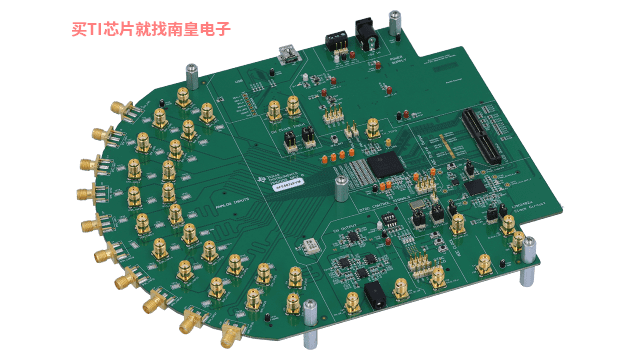
AFE5832EVM �� ���� LVDS �ӿں� CW ��Դ��Ƶ���� AFE5832 32 ͨ�������� AFE ����ģ��
AFE5832 ��һ��߶ȼ��ɵ�ģ��ǰ�� (AFE) ���������רΪ��Ҫʵ�ָ����ܵ�С�ߴ糬����ϵͳ����ơ�������������������ʱ��������� (TGC) ����·���������������� (CWD) ·������ 32 ͨ������֧�ָ��ֹ��ʺ�������ϣ���ʵ�����ϵͳ���ܡ���ˣ�AFE5832 ��һ�������ڸ߶˱�Яʽϵͳ�ij����� AFE ���������
AFE5832LP IBIS Model
PSpice for TI ���ṩ��������ģ���·���ܵ���ƺͷ��滷�����˹�����ȫ����ƺͷ�����ʹ�� Cadence ��ģ��������档PSpice for TI �����ʹ�ã�����ҵ�ڳ����ģ�Ϳ�֮һ���������ǵ�ģ��͵�Դ��Ʒϵ���Լ���ѡ��ģ����Ϊģ�͡�����?PSpice for TI ����ƺͷ��滷���������õ�ģ�Ϳ⣬���ɶԸ��ӵĻ���ź���ƽ��з��档�����������ն��豸��ƺ�ԭ�ͽ��������Ȼ���ٽ��в��ֺ����죬�����̲�Ʒ����ʱ�䲢���Ϳ����ɱ���
��?PSpice for TI ��ƺͷ��湤���У����������� TI (...)