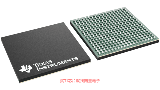
- 制造厂商:TI
- 产品类别:微控制器 (MCU) 和处理器
- 技术类目:处理器 - 基于 Arm 的处理器
- 功能描述:Sitara 处理器:Arm9,LPDDR,DDR2,显示,以太网,PROFIBUS
- 点击这里打开及下载AM1810的技术文档资料
- TI代理渠道,提供当日发货、严格的质量标准,满足您的目标价格

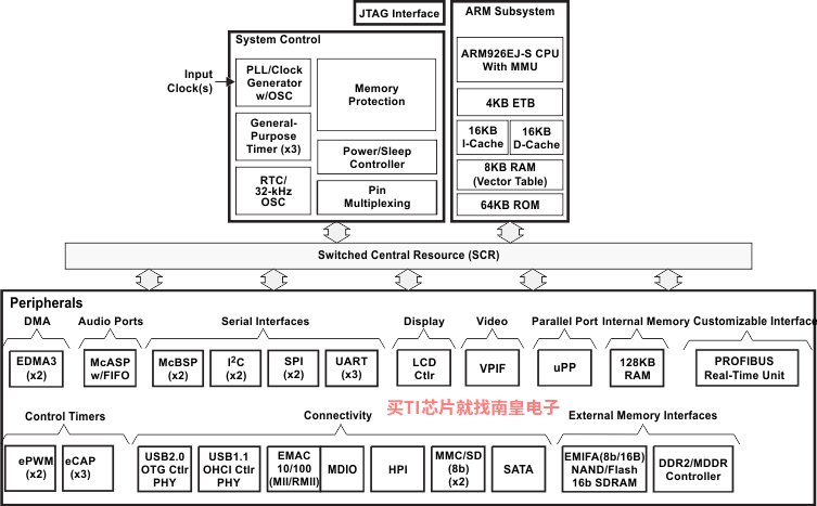
The AM1810 ARM Microprocessor for PROFIBUS is a low-power applications industrial processor based on ARM926EJ-S that is specifically targeted for PROFIBUS applications.
The device enables original-equipment manufacturers (OEMs) and original-design manufacturers (ODMs) to quickly bring to market devices featuring robust operating systems support, rich user interfaces, and high processing performance life through the maximum flexibility of a fully integrated mixed processor solution.
The ARM926EJ-S is a 32-bit RISC processor core that performs 32-bit or 16-bit instructions and processes 32-bit, 16-bit, or 8-bit data. The core uses pipelining so that all parts of the processor and memory system can operate continuously.
The ARM core has a coprocessor 15 (CP15), protection module, and data and program memory management units (MMUs) with table look-aside buffers. The ARM core processor has separate 16-KB instruction and 16-KB data caches. Both are four-way associative with virtual index virtual tag (VIVT). The ARM core also has 8KB of RAM (Vector Table) and 64KB of ROM.
The peripheral set includes: a 10/100 Mbps Ethernet media access controller (EMAC) with a management data input/output (MDIO) module; one USB2.0 OTG interface; one USB1.1 OHCI interface; two inter-integrated circuit (I2C Bus) interfaces; one multichannel audio serial port (McASP) with 16 serializers and FIFO buffers; two multichannel buffered serial ports (McBSPs) with FIFO buffers; two serial peripheral interfaces (SPIs) with multiple chip selects; four 64-bit general-purpose timers each configurable (one configurable as watchdog); a configurable 16-bit host-port interface (HPI); up to 9 banks of general-purpose input/output (GPIO) pins, with each bank containing 16 pins with programmable interrupt and event generation modes, multiplexed with other peripherals; three UART interfaces (each with RTS and CTS); two enhanced high-resolution pulse width modulator (eHRPWM) peripherals; three 32-bit enhanced capture (eCAP) module peripherals which can be configured as 3 capture inputs or 3 auxiliary pulse width modulator (APWM) outputs; two external memory interfaces; an asynchronous and SDRAM external memory interface (EMIFA) for slower memories or peripherals; and a higher speed DDR2/Mobile DDR controller.
The EMAC provides an efficient interface between the device and a network. The EMAC supports both 10Base-T and 100Base-TX, or 10 Mbps and 100 Mbps in either half- or full-duplex mode. Additionally, an MDIO interface is available for PHY configuration. The EMAC supports the MII and RMII interfaces.
The SATA controller provides a high-speed interface to mass data storage devices. The SATA controller supports SATA I (1.5 Gbps) and SATA II (3.0 Gbps).
The universal parallel port (uPP) provides a high-speed interface to many types of data converters, FPGAs or other parallel devices. The uPP supports programmable data widths between 8- to 16-bits on both channels. Single-data rate and double-data rate transfers are supported as well as START, ENABLE, and WAIT signals to provide control for a variety of data converters.
A video port interface (VPIF) is included providing a flexible video I/O port.
The rich peripheral set provides the ability to control external peripheral devices and communicate with external processors. For details on each of the peripherals, see the related sections in this document and the associated peripheral reference guides.
The device has a complete set of development tools for the ARM processor. These tools include C compilers, and scheduling, and a Windows debugger interface for visibility into source code execution.
- 375-MHz ARM926EJ-S RISC MPU
- ARM926EJ-S Core
- 32-Bit and 16-Bit (Thumb) Instructions
- Single-Cycle MAC
- ARM Jazelle Technology
- Embedded ICE-RT for Real-Time Debug
- ARM9 Memory Architecture
- 16KB of Instruction Cache
- 16KB of Data Cache
- 8KB of RAM (Vector Table)
- 64KB of ROM
- Enhanced Direct Memory Access Controller 3 (EDMA3):
- 2 Channel Controllers
- 3 Transfer Controllers
- 64 Independent DMA Channels
- 16 Quick DMA Channels
- Programmable Transfer Burst Size
- 128KB of On-Chip Memory
- 1.8-V or 3.3-V LVCMOS I/Os (Except for USB and DDR2 Interfaces)
- Two External Memory Interfaces:
- EMIFA
- NOR (8- or 16-Bit-Wide Data)
- NAND (8- or 16-Bit-Wide Data)
- 16-Bit SDRAM with 128-MB Address Space
- DDR2/Mobile DDR Memory Controller with one of the following:
- 16-Bit DDR2 SDRAM with 256-MB Address Space
- 16-Bit mDDR SDRAM with 256-MB Address Space
- EMIFA
- Three Configurable 16550-Type UART Modules:
- With Modem Control Signals
- 16-Byte FIFO
- 16x or 13x Oversampling Option
- LCD Controller
- Two Serial Peripheral Interfaces (SPIs) Each with Multiple Chip Selects
- Two Multimedia Card (MMC)/Secure Digital (SD) Card Interfaces with Secure Data I/O (SDIO) Interfaces
- Two Master and Slave Inter-Integrated Circuits (I2C Bus)
- One Host-Port Interface (HPI) with 16-Bit-Wide Muxed Address and Data Bus For High Bandwidth
- Programmable Real-Time Unit Subsystem (PRUSS) with PROFIBUS
- Two Independent Programmable Real-Time Unit (PRU) Cores
- 32-Bit Load-Store RISC Architecture
- 4KB of Instruction RAM per Core
- 512 Bytes of Data RAM per Core
- PRUSS can be Disabled via Software to Save Power
- Register 30 of Each PRU is Exported from the Subsystem in Addition to the Normal R31 Output of the PRU Cores.
- Standard Power-Management Mechanism
- Clock Gating
- Entire Subsystem Under a Single PSC Clock Gating Domain
- Dedicated Interrupt Controller
- Dedicated Switched Central Resource
- Two Independent Programmable Real-Time Unit (PRU) Cores
- USB 1.1 OHCI (Host) with Integrated PHY (USB1)
- USB 2.0 OTG Port with Integrated PHY (USB0)
- USB 2.0 High- and Full-Speed Client
- USB 2.0 High-, Full-, and Low-Speed Host
- End Point 0 (Control)
- End Points 1,2,3,4 (Control, Bulk, Interrupt or ISOC) RX and TX
- One Multichannel Audio Serial Port (McASP):
- Transmit and Receive Clocks
- Two Clock Zones and 16 Serial Data Pins
- Supports TDM, I2S, and Similar Formats
- DIT-Capable
- FIFO Buffers for Transmit and Receive
- Two Multichannel Buffered Serial Ports (McBSPs):
- Transmit and Receive Clocks
- Supports TDM, I2S, and Similar Formats
- AC97 Audio Codec Interface
- Telecom Interfaces (ST-Bus, H100)
- 128-Channel TDM
- FIFO Buffers for Transmit and Receive
- 10/100 Mbps Ethernet MAC (EMAC):
- IEEE 802.3 Compliant
- MII Media-Independent Interface
- RMII Reduced Media-Independent Interface
- Management Data I/O (MDIO) Module
- Video Port Interface (VPIF):
- Two 8-Bit SD (BT.656), Single 16-Bit or Single Raw (8-, 10-, and 12-Bit) Video Capture Channels
- Two 8-Bit SD (BT.656), Single 16-Bit Video Display Channels
- Universal Parallel Port (uPP):
- High-Speed Parallel Interface to FPGAs and Data Converters
- Data Width on Both Channels is 8- to 16-Bit Inclusive
- Single-Data Rate or Dual-Data Rate Transfers
- Supports Multiple Interfaces with START, ENABLE, and WAIT Controls
- Serial ATA (SATA) Controller:
- Supports SATA I (1.5 Gbps) and SATA II (3.0 Gbps)
- Supports all SATA Power Management Features
- Hardware-Assisted Native Command Queueing (NCQ) for up to 32 Entries
- Supports Port Multiplier and Command-Based Switching
- Real-Time Clock (RTC) with 32-kHz Oscillator and Separate Power Rail
- Three 64-Bit General-Purpose Timers (Each Configurable as Two 32-Bit Timers)
- One 64-Bit General-Purpose or Watchdog Timer (Configurable as Two 32-Bit General-Purpose Timers)
- Two Enhanced High-Resolution Pulse Width Modulators (eHRPWMs):
- Dedicated 16-Bit Time-Base Counter with Period and Frequency Control
- 6 Single-Edge Outputs, 6 Dual-Edge Symmetric Outputs, or 3 Dual-Edge Asymmetric Outputs
- Dead-Band Generation
- PWM Chopping by High-Frequency Carrier
- Trip Zone Input
- Three 32-Bit Enhanced Capture (eCAP) Modules:
- Configurable as 3 Capture Inputs or 3 Auxiliary Pulse Width Modulator (APWM) Outputs
- Single-Shot Capture of up to Four Event Time-Stamps
- 361-Ball Pb-Free PBGA [ZWT Suffix], 0.80-mm Ball Pitch
- Extended Temperature
- Arm CPU
- 1 Arm9
- Arm MHz (Max.)
- 375, 456
- Co-processor(s)
- PRU-ICSS
- CPU
- 32-bit
- Display type
- 1 LCD
- Protocols
- Ethernet, Profibus
- Ethernet MAC
- 1-Port 10/100
- Hardware accelerators
- PRUSS
- Operating system
- Linux, RTOS
- Security
- Device identity, Memory protection
- Rating
- Catalog
- Power supply solution
- TPS650061
- Operating temperature range (C)
- -40 to 105
AM1810的完整型号有:AM1810EZWTA3,以下是这些产品的关键参数及官网采购报价:
AM1810EZWTA3,工作温度:-40 to 105,封装:NFBGA (ZWT)-361,包装数量MPQ:90个,MSL 等级/回流焊峰值温度:Level-3-260C-168 HR,引脚镀层/焊球材料:SNAGCU,TI官网AM1810EZWTA3的批量USD价格:16.31(1000+)

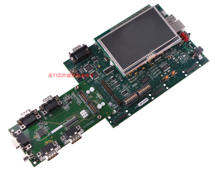
TMDXEVM1810 ― AM1810 Profibus 评估模块
AM1810 评估模块 (EVM) 是一款全功能的应用程序开发套件,用于评估德州仪器 (TI) 高度集成的节能型 AM1810 Sitara ARM 处理器的功能。
AM1810 处理器是工业、便携式医疗、通信和消费者市场等领域的应用的理想选择。特别地,AM1810 处理器在芯片上集成了 PROFIBUS 工业通信接口,因此无需借助外部 PROFIBUS 器件。AM1810 EVM 提供的单一开发环境可让客户评估和使用包括 PROFIBUS 接口在内的所有外设。
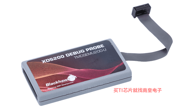
TMDSEMU200-U ― Spectrum Digital XDS200 USB 仿真器
Spectrum Digital XDS200 是最新 XDS200 系列 TI 处理器调试探针(仿真器)的首个模型。XDS200 系列拥有超低成本 XDS100 与高性能 XDS560v2 之间的低成本与高性能的完美平衡。此外,对于带有嵌入式缓冲跟踪器 (ETB) 的所有 ARM 和 DSP 处理器,所有 XDS 调试探针均支持内核和系统跟踪。
Spectrum Digital XDS200 通过 TI 20 引脚连接器(带有适合 TI 14 引脚、TI 10 引脚和 ARM 20 引脚的多个适配器)连接到目标板,而通过 USB2.0 高速连接 (480Mbps) 连接到主机 PC。要在主机 (...)
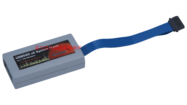
TMDSEMU560V2STM-U ― Blackhawk XDS560v2 系统跟踪 USB 仿真器
XDS560v2 System Trace 是 XDS560v2 系列高性能 TI 处理器调试探针(仿真器)的第一种型号。XDS560v2 是 XDS 系列调试探针中性能最高的一款,同时支持传统 JTAG 标准 (IEEE1149.1) 和 cJTAG (IEEE1149.7)。
XDS560v2 System Trace 在其巨大的外部存储器缓冲区中加入了系统引脚跟踪。这种外部存储器缓冲区适用于指定的 TI 器件,通过捕获相关器件级信息,获得准确的总线性能活动和吞吐量,并对内核和外设进行电源管理。此外,对于带有嵌入式缓冲跟踪器 (ETB) 的所有 ARM 和 DSP 处理器,所有 XDS (...)
TMDSEMU560V2STM-UE ― Spectrum Digital XDS560v2 系统跟踪 USB 和以太网
XDS560v2 System Trace 是 XDS560v2 系列高性能 TI 处理器调试探针(仿真器)的第一种型号。XDS560v2 是 XDS 系列调试探针中性能最高的一款,同时支持传统 JTAG 标准 (IEEE1149.1) 和 cJTAG (IEEE1149.7)。
XDS560v2 System Trace 在其巨大的外部存储器缓冲区中加入了系统引脚跟踪。这种外部存储器缓冲区适用于指定的 TI 器件,通过捕获相关器件级信息,获得准确的总线性能活动和吞吐量,并对内核和外设进行电源管理。此外,对于带有嵌入式缓冲跟踪器 (ETB) 的所有 ARM 和 DSP 处理器,所有 XDS (...)
LINUXEZSDK-AM18X — 用于 AM1808、AM1806 和 AM1802 的 Linux EZ SDK
PROFIBUS(过程现场总线)是世界上最成功的工业自动化现场总线(通信)技术,由 PROFIBUS and PROFINET International (PNO/PI) 组织监管。PROFIBUS 是一种广泛部署的技术,截止到 2009 年末,已经安装了 3 千万以上的 PROFIBUS 节点,并且目前的年增长率为 10% 左右。通过更好的控制和在线诊断,PROFIBUS 可以改善资产管理,确保更低的生命周期成本、更好的质量和更高的生产力。德州仪器公司 (TI) 已将 PROFIBUS 功能集成到了其 AM1810 Sitara ARM 微处理器 (MPU) 和 (...)
CCSTUDIO-SITARA ― 适用于 Sitara™ 处理器的 Code Composer Studio (CCS) 集成开发环境 (IDE)
Code Composer Studio™ - Integrated Development Environment for Sitara™ ARM© ProcessorsCode Composer Studio is an integrated development environment (IDE) that supports TI's Microcontroller and Embedded Processors portfolio. Code Composer Studio comprises a suite of tools used to develop and debug (...)
AM1810 ZWT BSDL Model
TI has partnered with companies to offer a wide range of software, tools, and SOMs using TI processors to accelerate your path to production. Download this search tool to quickly browse our third-party solutions and find the right third-party to meet your needs. The software, tools and modules (...)