- ���쳧�̣�TI
- ��Ʒ������͵�ѹת��
- ������Ŀ�����������������ͼĴ��� - ��λ�Ĵ���
- ���������������� CMOS 8 ����̬��λ�Ĵ���
- ������������CD4021B-Q1�ļ����ĵ�����
- TI�����������ṩ���շ������ϸ������������������Ŀ��۸�

CD4021B series types are 8-stage parallel- or serial-input/serial output registers having common CLOCK and PARALLEL/SERIAL CONTROL inputs, a single SERIAL data input, and individual parallel "JAM" inputs to each register stage. Each register stage is a D-type, master-slave flip-flop. In addition to an output from stage 8, "Q" outputs are also available from stages 6 and 7. Parallel as well as serial entry is made into the register synchronously with the positive clock line transition in the CD4014B. In the CD4021B serial entry is synchronous with the clock but parallel entry is asynchronous. In both types, entry is controlled by the PARALLEL/SERIAL CONTROL input. When the PARALLEL/SERIAL CONTROL input is low, data is serially shifted into the 8-stage register synchronously with the positive transition of the clock line. When the PARALLEL/SERIAL CONTROL input is high, data is jammed into the 8-stage register via the parallel input lines and synchronous with the positive transition of the clock line. In the CD4021B, the CLOCK input of the internal stage is "forced" when asynchronous parallel entry is made. Register expansion using multiple packages is permitted.
The CD4021B series types are supplied in 16-lead hermetic dual-in-line ceramic packages (D and F suffixes), 16-lead dual-in-line plastic packages (E suffix), and in chip form (H suffix).
- Qualified for Automotive Applications
- Medium-Speed Operation: 12-MHz (Typ) Clock Rate at VDD �C VSS = 10 V
- Fully Static Operation
- Eight Master-Slave Flip-Flops Plus Output Buffering and Control Gating
- 100% Tested for Quiescent Current at 20 V
- Maximum Input Current of 1 ��A at 18 V Over Full Package-Temperature Range: 100 nA at 18 V and 25��C
- Noise Margin (Full Package-Temperature Range):
- 1 V at VDD = 5 V
- 2 V at VDD = 10 V
- 2.5 V at VDD = 15 V
- Standardized Symmetrical Output Characteristics
- 5-V, 10-V, and 15-V Parametric Ratings
- Meets All Requirements of JEDEC Tentative Standard No. 13B, "Standard Specifications for Description of ��B�� Series CMOS Devices"
- Latch-Up Performance Meets 50 mA per JESD 78, Class I
- APPLICATIONS
- Parallel Input/Serial Output Data Queuing
- Parallel-to-Serial Data Conversion
- General-Purpose Register
- Configuration
- Serial-in, Parallel-out
- Bits (#)
- 8
- Technology Family
- CD4000
- Supply voltage (Min) (V)
- 3
- Supply voltage (Max) (V)
- 18
- Input type
- Standard CMOS
- Output type
- Push-Pull
- Clock Frequency (MHz)
- 8.5
- IOL (Max) (mA)
- 4.2
- IOH (Max) (mA)
- -4.2
- ICC (Max) (uA)
- 3000
- Features
- Balanced outputs, Standard speed (tpd > 50ns), Positive input clamp diode
CD4021B-Q1�������ͺ��У�CD4021BQDRQ1����������Щ��Ʒ�Ĺؼ������������ɹ����ۣ�
CD4021BQDRQ1�������¶ȣ�-40 to 125����װ��SOIC (D)-16����װ����MPQ��2500����MSL �ȼ�/��������ֵ�¶ȣ�Level-1-260C-UNLIM�����ŶƲ�/������ϣ�NIPDAU��TI����CD4021BQDRQ1������USD�۸�.173��1000+��

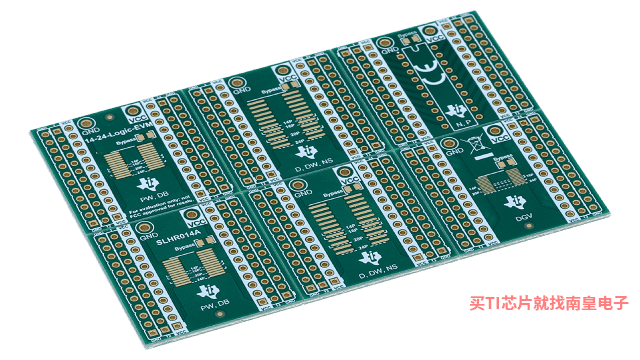
14-24-LOGIC-EVM �� ֧�� 14 �� 24 ���� PW��DB��D��DW��NS��DYY �� DGV ��װ��ͨ���� EVM
�� EVM �������֧�ֲ��� 14 �� 24 ���� D��DW��DB��NS��PW��DYY �� DGV ��װ���κ���������