- 制造厂商:TI
- 产品类别:逻辑和电压转换
- 技术类目:触发器、锁存器和寄存器 - 移位寄存器
- 功能描述:CMOS 8 级静态双向并行/串行输入/输出总线寄存器
- 点击这里打开及下载CD4034B的技术文档资料
- TI代理渠道,提供当日发货、严格的质量标准,满足您的目标价格

CD4034B is a static eight-stage parallel-or serial-input parallel-output register. It can be used to:
1) bidirectionally transfer parallel information between two buses, 2) convert serial data to parallel form and direct the parallel data to either of two buses, 3) store (recirculate) parallel data, or 4) accept parallel data from either of two buses and convert that data to serial form. Input that control the operations include a single-phase CLOCK (CL), A DATA ENABLE (AE), ASYNCHRONOUS/SYNCHRONOUS (A/S), A-BUS-TO-B-BUS/B-BUS-TO-A-BUS (A/B), and PARALLEL/SERIAL (P/S).
Data inputs include 16 bidirectional parallel data lines of which the eight A data lines are inputs (3-state outputs) and the B data lines are outputs (inputs) depending on the signal level on the A/B input. In addition, an input for SERIAL DATA is also provided.
All register stages are D-type master-slave flip-flops with separate master and slave clock inputs generated internally to allow synchronous or asynchronous data transfer from master to slave. Isolation from external noise and the effects of loading is provided by output buffering.
Register expansion can be accomplished by simply cascading CD4034B packages.
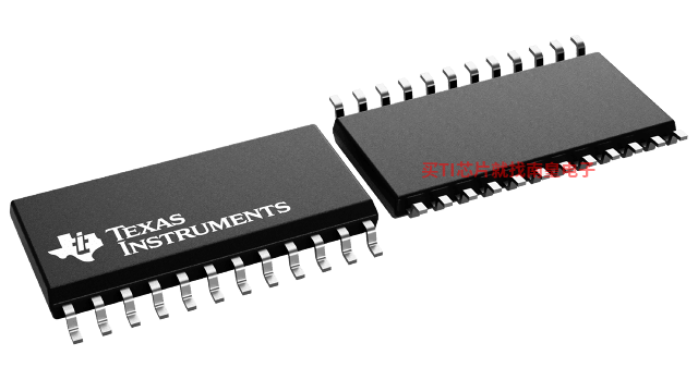
The CD4034B types are supplied in 24-lead hermetic dual-in-line ceramic packages (F3A suffix), 24-lead dual-in-line plastic packages (E suffix), 24-lead small-outline packages (M, M96, and NSR suffixes), and 24-lead thin shrink small-outline packages (PW and PWR suffixes).
- Bidirectional parallel data input
- Parallel or serial inputs/parallel outputs
- Asynchronous or synchronous parallel data loading
- Parallel data-input enable on "A" data lines (3-state output)
- Data recirculation for register expansion
- Multipackage register expansion
- Fully static operation dc-to-10 MHz (typ.) at VDD = 10 V
- Standardized, symmetrical output characteristics
- 100% tested for quiescent current at 20 V
- 5-V, 10-V, and 15-V parametric ratings
- Maximum input current of 1 μA at 18 V over full package-temperature range; 100nA at 18 V and 25°C
- Noise margin (over full package-temperature range):
- 1 V at VDD = 5 V
- 2 V at VDD = 10 V
- 2.5 V at VDD = 15 V
- Meets all requirements of JEDEC Tentative Standard No. 13A, "Standard Specifications for Description of 'B' Series CMOS Devices"
- Applications:
- Parallel Input/Parallel Output, Serial Input/Parallel Output, Serial Input/Serial Output Register
- Shift right/shift left register
- Shift right/shift left with parallel loading
- Address register
- Buffer register
- Bus system register with enable parallel lines at bus side
- Double bus register system
- Up-Down Johnson or ring counter
- Pseudo-random code generators
- Sample and hold register (storage, counting, display)
- Frequency and phase comparator
- Configuration
- Universal
- Bits (#)
- 8
- Technology Family
- CD4000
- Supply voltage (Min) (V)
- 3
- Supply voltage (Max) (V)
- 18
- Input type
- Standard CMOS
- Output type
- Push-Pull
- Clock Frequency (MHz)
- 8.5
- IOL (Max) (mA)
- 4.2
- IOH (Max) (mA)
- -4.2
- ICC (Max) (uA)
- 3000
- Features
- Balanced outputs, Standard speed (tpd > 50ns), Positive input clamp diode
CD4034B的完整型号有:CD4034BM,以下是这些产品的关键参数及官网采购报价:
CD4034BM,工作温度:-55 to 125,封装:SOIC (DW)-24,包装数量MPQ:25个,MSL 等级/回流焊峰值温度:Level-1-260C-UNLIM,引脚镀层/焊球材料:NIPDAU,TI官网CD4034BM的批量USD价格:.448(1000+)

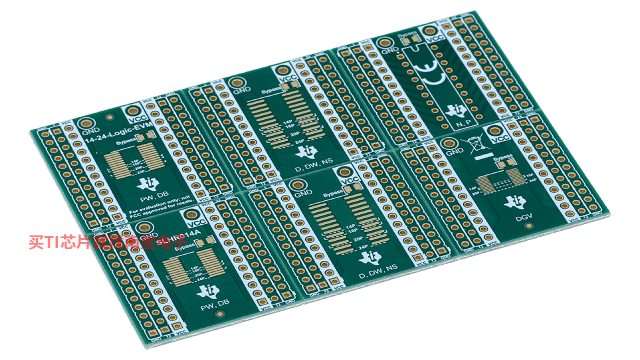
14-24-LOGIC-EVM ― 支持 14 到 24 引脚 PW、DB、D、DW、NS、DYY 和 DGV 封装的通用逻辑 EVM
该 EVM 设计用于支持采用 14 至 24 引脚 D、DW、DB、NS、PW、DYY 或 DGV 封装的任何逻辑器件。