- ���쳧�̣�TI
- ��Ʒ����������·������
- ������Ŀ��ģ��غͶ�·������
- ���������������� 20V��1:1 (SPST)��4 ͨ��ģ���
- ������������CD4066B-Q1�ļ����ĵ�����
- TI�����������ṩ���շ������ϸ������������������Ŀ��۸�

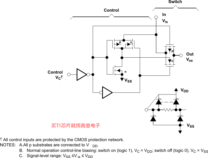
The CD4066B-Q1 is a quad bilateral switch intended for the transmission or multiplexing of analog or digital signals. It is pin-for-pin compatible with the CD4016B, but exhibits a much lower on-state resistance. In addition, the on-state resistance is relatively constant over the full signal-input range.
The CD4066B-Q1 consists of four bilateral switches, each with independent controls. Both the p and the n devices in a given switch are biased on or off simultaneously by the control signal. As shown in , the well of the n-channel device on each switch is tied to either the input (when the switch is on) or to VSS (when the switch is off). This configuration eliminates the variation of the switch-transistor threshold voltage with input signal and, thus, keeps the on-state resistance low over the full operating-signal range.
The advantages over single-channel switches include peak input-signal voltage swings equal to the full supply voltage and more constant on-state impedance over the input-signal range. However, for sample-and-hold applications, the CD4016B is recommended.
- Qualified for Automotive Applications
- 15-V Digital or ��7.5-V Peak-to-Peak Switching
- 125-�� Typical On-State Resistance for 15-V Operation
- Switch On-State Resistance Matched to Within 5 �� Over 15-V Signal-Input Range
- On-State Resistance Flat Over Full Peak-to-Peak Signal Range
- High On/Off Output-Voltage Ratio: 80 dB Typical at fis = 10 kHz, RL = 1 k?
- High Degree of Linearity: <0.5% Distortion Typical at fis = 1 kHz, Vis = 5 V p-p, VDD �C VSS �� 10 V, RL = 10 k��
- Extremely Low Off-State Switch Leakage, Resulting in Very Low Offset Current and High Effective Off-State Resistance: 10 pA Typical at VDD �C VSS = 10 V, TA = 25��C
- Extremely High Control Input Impedance (Control Circuit Isolated From Signal Circuit): 1012 �� Typical
- Low Crosstalk Between Switches: �C50 dB Typical at fis = 8 MHz, RL = 1 k��
- Matched Control-Input to Signal-Output Capacitance: Reduces Output Signal Transients
- Frequency Response, Switch On = 40 MHz Typical
- 100% Tested for Quiescent Current at 20 V
- 5-V, 10-V, and 15-V Parametric Ratings
- Latch-Up Exceeds 100mA per JESD78 - Class I
- Meets All Requirements of JEDEC Tentative Standard No. 13-B, Standard Specifications for Description of "B" Series CMOS Devices
- APPLICATIONS
- Analog Signal Switching/Multiplexing: Signal Gating, Modulator, Squelch Control, Demodulator, Chopper, Commutating Switch
- Digital Signal Switching/Multiplexing
- Transmission-Gate Logic Implementation
- Analog-to-Digital and Digital-to-Analog Conversion
- Digital Control of Frequency, Impedance, Phase, and Analog-Signal Gain
- Configuration
- 1:1 SPST
- Number of channels (#)
- 4
- Power supply voltage - single (V)
- 3.3, 5, 12, 16, 20
- Protocols
- Analog
- Ron (Typ) (Ohms)
- 125
- CON (Typ) (pF)
- 8
- Bandwidth (MHz)
- 40
- Operating temperature range (C)
- -40 to 125
- Input/output continuous current (Max) (mA)
- 10
- Rating
- Automotive
- Supply current (Typ) (uA)
- 0.01
CD4066B-Q1�������ͺ��У�CD4066BQDRQ1����������Щ��Ʒ�Ĺؼ������������ɹ����ۣ�
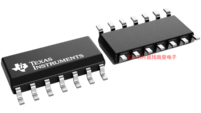
CD4066BQDRQ1�������¶ȣ�-40 to 125����װ��SOIC (D)-14����װ����MPQ��2500����MSL �ȼ�/��������ֵ�¶ȣ�Level-1-260C-UNLIM�����ŶƲ�/������ϣ�NIPDAU��TI����CD4066BQDRQ1������USD�۸�.14��1000+��

LEADED-ADAPTER1 �� ���ڿ��ٲ��� TI 5��8��10��16 �� 24 ��������ʽ��װ�ı�����װת DIP ��ͷ������
EVM-LEADED1 ��ɶ� TI �ij�������ʽ��װ���п��ٲ��Ժ͵�·�����顣������������㹻�Ŀռ䣬�ɽ� TI �� D��DBQ��DCT��DCU��DDF��DGS��DGV �� PW ������װ��װת��Ϊ 100mil DIP ��ͷ��