- 制造厂商:TI
- 产品类别:逻辑和电压转换
- 技术类目:触发器、锁存器和寄存器 - 移位寄存器
- 功能描述:CMOS 8 级移位存储总线寄存器
- 点击这里打开及下载CD4094B的技术文档资料
- TI代理渠道,提供当日发货、严格的质量标准,满足您的目标价格

CD4094B is an 8-stage serial shift register having a storage latch associated with each stage for strobing data from the serial input to parallel buffered 3-state outputs. The parallel outputs may be connected directly to common bus lines. Data is shifted on positive clock transitions. The data in each shift register stage is transferred to the storage register when the STROBE input is high. Data in the storage register appears at the outputs whenever the OUTPUT-ENABLE signal is high.
Two serial outputs are available for cascading a number of CD4094B devices. Data is available at the QS serial output terminal on positive clock edges to allow for high-speed operation in cascaded systems in which the clock rise time is fast. The same serial information, available at the Q'S terminal on the next negative clock edge, provides a means for cascading CD4094B devices when the clock rise time is slow.
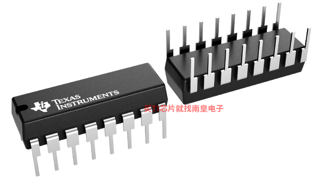
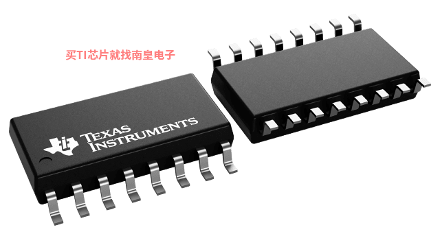
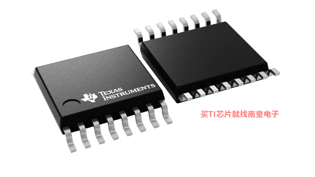
The CD4094B types are supplied in 16-lead hermetic dual-in-line ceramic packages (F3A suffix), 16-lead dual-in-line plastic packages (E suffix), 16-lead small-outline packages (NSR suffix), and 16-lead thin shrink small-outline packages (PW and PWR suffixes).
- 3-state parallel outputs for connection to common bus
- Separate serial outputs synchronous to both positive and negative clock edges for cascading
- Medium speed operation - 5 MHz at 10 V (typ.)
- Standardized, symmetrical output characteristics
- 100% tested for quiescent current at 20 V
- Maximum input current of 1 μA at 18 V over full package-temperature range; 100 nA at 18 V and 25°C
- Noise margin (full package temperature range): 1 V at VDD = 5 V 2 V at VDD = 10 V 2.5 V at VDD = 15 V
- 5-V, 10-V, and 15-V parametric ratings
- Meets all requirements of JEDEC Tentative Standard No. 13B, "Standard Specifications for Description of 'B' Series CMOS Devices"
- Applications
- Serial-to-parallel data conversion
- Remote control holding register
- Dual-rank shift, hold, and bus applications
- Configuration
- Serial-in, Parallel-out
- Bits (#)
- 8
- Technology Family
- CD4000
- Supply voltage (Min) (V)
- 3
- Supply voltage (Max) (V)
- 18
- Input type
- Standard CMOS
- Output type
- Push-Pull
- Clock Frequency (MHz)
- 3
- IOL (Max) (mA)
- 4.2
- IOH (Max) (mA)
- -4.2
- ICC (Max) (uA)
- 3000
- Features
- Balanced outputs, Standard speed (tpd > 50ns), Positive input clamp diode
CD4094B的完整型号有:CD4094BE、CD4094BNSR、CD4094BPW、CD4094BPWR,以下是这些产品的关键参数及官网采购报价:
CD4094BE,工作温度:-55 to 125,封装:PDIP (N)-16,包装数量MPQ:25个,MSL 等级/回流焊峰值温度:N/A for Pkg Type,引脚镀层/焊球材料:NIPDAU,TI官网CD4094BE的批量USD价格:.133(1000+)
CD4094BNSR,工作温度:-55 to 125,封装:SO (NS)-16,包装数量MPQ:2000个,MSL 等级/回流焊峰值温度:Level-1-260C-UNLIM,引脚镀层/焊球材料:NIPDAU,TI官网CD4094BNSR的批量USD价格:.127(1000+)
CD4094BPW,工作温度:-55 to 125,封装:TSSOP (PW)-16,包装数量MPQ:90个,MSL 等级/回流焊峰值温度:Level-1-260C-UNLIM,引脚镀层/焊球材料:NIPDAU,TI官网CD4094BPW的批量USD价格:.306(1000+)
CD4094BPWR,工作温度:-55 to 125,封装:TSSOP (PW)-16,包装数量MPQ:2000个,MSL 等级/回流焊峰值温度:Level-1-260C-UNLIM,引脚镀层/焊球材料:NIPDAU,TI官网CD4094BPWR的批量USD价格:.121(1000+)

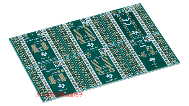
14-24-LOGIC-EVM ― 支持 14 到 24 引脚 PW、DB、D、DW、NS、DYY 和 DGV 封装的通用逻辑 EVM
该 EVM 设计用于支持采用 14 至 24 引脚 D、DW、DB、NS、PW、DYY 或 DGV 封装的任何逻辑器件。