- 制造厂商:TI
- 产品类别:逻辑和电压转换
- 技术类目:触发器、锁存器和寄存器 - 其他锁存器
- 功能描述:CMOS 8 位可寻址锁存器
- 点击这里打开及下载CD4099B的技术文档资料
- TI代理渠道,提供当日发货、严格的质量标准,满足您的目标价格

CD4099B 8-bit addressable latch is a serial-input, parallel-output storage register that can perform a variety of functions.
Data are inputted to a particular bit in the latch when that bit is addressed (by means of input A0, A1, A2) and when WRITE DISABLE is at a low level. When WRITE DISABLE is high, data entry is inhibited; however, all 8 outputs can be continuously read independent of WRITE DISABLE and address inputs.
A master RESET input is available, which resets all bits to a logic "0" level when RESET and WRITE DISABLE are at a high level. When RESET is at a high level, and WRITE RESET is at a low level, the latch acts as a 1-of-8 demultiplexer; the bit that is addressed has an active output which follows the data input, while all unaddressed bits are held to a logic "0" level.
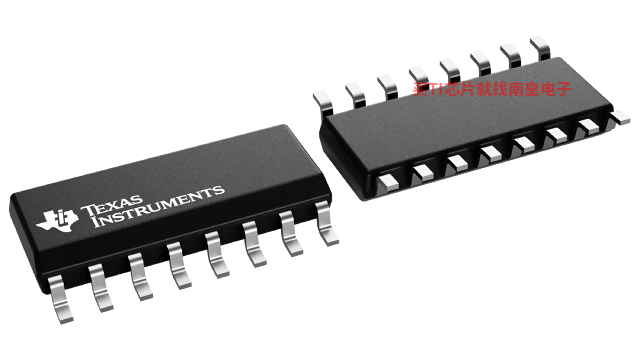
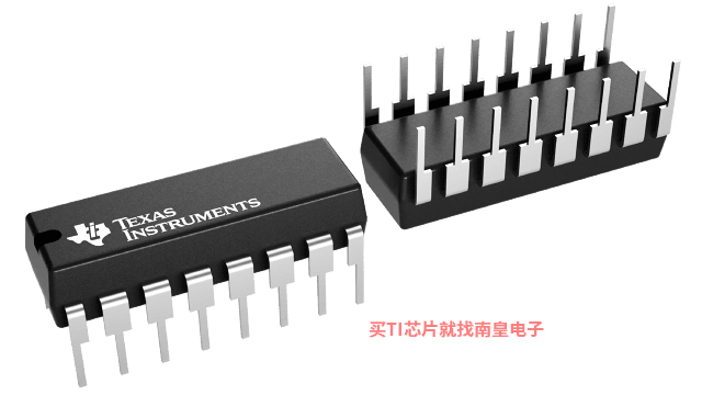
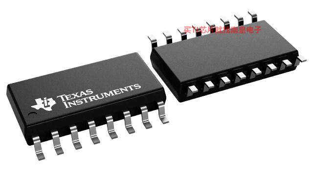
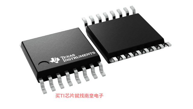
The CD4099B types are supplied in 16-lead hermetic dual-in-line ceramic packages (F3A suffix), 16-lead dual-in-line plastic package (E suffix), 16-lead small-outline package (M, M96, MT, and NSR suffixes), and 16-lead thin shrink small-outline packages (PW and PWR suffixes).
- Serial data input
- Active parallel output
- Storage register capability
- Master clear
- Can function as demultiplexer
- Standardized, symmetrical output characteristics
- 100% tested for quiescent current at 20 V
- Maximum input current of 1 uA at 18 V over full package-temperature range; 100 nA at 18 V and 25°C
- Noise margin (full package-temperature range) = 1 V at VDD = 5 V 2 V at VDD = 10 V 2.5 V at VDD = 15 V
- 5-V, 10-V, and 15-V parametric ratings
- Meets all requirements of JEDEC Tentative Standard No. 13B, "Standard Specifications for Description of ’B’ Series CMOS Devices"
- Applications:
- Multi-line decoders
- A/D converters
- Function
- Addressable Latch
- Number of channels (#)
- 8
- Technology Family
- CD4000
- Supply voltage (Min) (V)
- 3
- Supply voltage (Max) (V)
- 18
- Input type
- Standard CMOS
- Output type
- Push-Pull
- Data rate (Max) (Mbps)
- 16
- IOL (Max) (mA)
- 2.4
- IOH (Max) (mA)
- -2.4
- Features
- Standard speed (tpd > 50ns), High speed (tpd 10-50ns), Partial power down (Ioff)
CD4099B的完整型号有:CD4099BE、CD4099BM、CD4099BM96、CD4099BNSR、CD4099BPWR,以下是这些产品的关键参数及官网采购报价:
CD4099BE,工作温度:-55 to 125,封装:PDIP (N)-16,包装数量MPQ:25个,MSL 等级/回流焊峰值温度:N/A for Pkg Type,引脚镀层/焊球材料:NIPDAU,TI官网CD4099BE的批量USD价格:0.192(1000+)
CD4099BM,工作温度:-55 to 125,封装:SOIC (D)-16,包装数量MPQ:40个,MSL 等级/回流焊峰值温度:Level-1-260C-UNLIM,引脚镀层/焊球材料:NIPDAU,TI官网CD4099BM的批量USD价格:0.367(1000+)
CD4099BM96,工作温度:-55 to 125,封装:SOIC (D)-16,包装数量MPQ:2500个,MSL 等级/回流焊峰值温度:Level-1-260C-UNLIM,引脚镀层/焊球材料:NIPDAU,TI官网CD4099BM96的批量USD价格:0.126(1000+)
CD4099BNSR,工作温度:-55 to 125,封装:SO (NS)-16,包装数量MPQ:2000个,MSL 等级/回流焊峰值温度:Level-1-260C-UNLIM,引脚镀层/焊球材料:NIPDAU,TI官网CD4099BNSR的批量USD价格:0.183(1000+)
CD4099BPWR,工作温度:-55 to 125,封装:TSSOP (PW)-16,包装数量MPQ:2000个,MSL 等级/回流焊峰值温度:Level-1-260C-UNLIM,引脚镀层/焊球材料:NIPDAU,TI官网CD4099BPWR的批量USD价格:0.167(1000+)

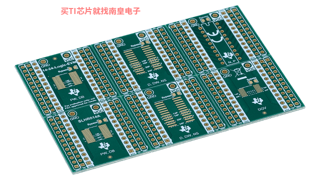
14-24-LOGIC-EVM ― 支持 14 到 24 引脚 PW、DB、D、DW、NS、DYY 和 DGV 封装的通用逻辑 EVM
该 EVM 设计用于支持采用 14 至 24 引脚 D、DW、DB、NS、PW、DYY 或 DGV 封装的任何逻辑器件。
