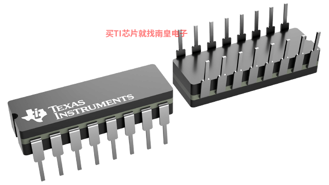
- 制造厂商:TI
- 产品类别:逻辑和电压转换
- 技术类目:专用逻辑 IC - 数字计时 IC
- 功能描述:CMOS 可编程计时器
- 点击这里打开及下载CD4536B-MIL的技术文档资料
- TI代理渠道,提供当日发货、严格的质量标准,满足您的目标价格

CD4536B is a programmable timer consisting of 24 ripple-binary counter stages. The salient feature of this device is its flexibility. The device can count from 1 to 224 or the first 8 stages can be bypassed to allow an output, selectable by a 4-bit code, from any one of the remaining 16 stages. It can be driven by an external clock or an RC oscillator that can be constructed using on-chip components. Input IN1 serves as either the external clock input or the input to the on-chip RC oscillator. OUT1 and OUT2 are connection terminals for the external RC components. In addition, an on-chip monostable circuit is provided to allow a variable pulse width output. Various timing functions can be achieved using combinations of these capabilities.
A logic 1 on the 8-BYPASS input enables a bypass of the first 8 stages and makes stage 9 the first counter stage of the last 16 stages. Selection of 1 of 16 outputs is accomplished by the decoder and the BCD inputs A, B, C and D. MONO IN is the timing input for the on-chip monostable oscillator. Grounding of the MONO IN terminal through a resistor of 10K ohms or higher, disables the one-shot circuit and connects the decoder directly to the DECODE OUT terminal. A resistor to VDD and a capacitor to ground from the MONO IN terminal enables the one-shot circuit and control its pulse width.
A fast test mode is enabled by a logic 1 on 8-BYPASS, SET, and RESET. This mode divides the 24-stage counter into three 8-stage sections to facilitate a fast test sequence.
The CD4536B types are supplied in 16-lead hermetic dual-in-line ceramic packages (F3A suffix), 16-lead dual-in-line plastic packages (E suffix), 16-lead small-outline packages (DW, DWR, and NSR suffixes), and 16-lead thin shrink small-outline packages (PW and PWR suffixes).
- 24 flip-flop stages - - counts from 20 to 224
- Last 16 stages selectable by BCD select code
- Bypass input allows bypassing first 8 stages
- On-chip RC oscillator provision
- Clock inhibit input
- Schmitt-trigger in clock line permits operation with very long rise and fall times
- On-chip monostable output provision
- Typical fCL = 3 MHz at VDD = 10 V
- Test mode allows fast test sequence
- Set and reset inputs
- Capable of driving two low power TTL loads, one lower-power Schottky load, or two HTL loads over the rated temperature range
- Standardized, symmetrical output characteristics
- 100% tested for quiescent current at 20 V
- 5-V, 10-V, and 15-V parametric ratings
- Meets all requirements of JEDEC Tentative Standard No. 13B, "Standard Specifications for Description of ’B’ Series CMOS Devices"
- Technology Family
- CD4000
- Bits (#)
- 4
- Supply voltage (Min) (V)
- 3
- Supply voltage (Max) (V)
- 18
- Input type
- Standard CMOS
- Output type
- Push-Pull
- ICC (Max) (uA)
- 100
- IOL (Max) (mA)
- 4
- IOH (Max) (mA)
- -4
CD4536B-MIL的完整型号有:CD4536BF3A,以下是这些产品的关键参数及官网采购报价:
CD4536BF3A,工作温度:-55 to 125,封装:CDIP (J)-16,包装数量MPQ:1个,MSL 等级/回流焊峰值温度:N/A for Pkg Type,引脚镀层/焊球材料:SNPB,TI官网CD4536BF3A的批量USD价格:11.781(1000+)

CD4536BF3A,工作温度:-55 to 125,封装:CDIP (J)-16,包装数量MPQ:1个,MSL 等级/回流焊峰值温度:N/A for Pkg Type,引脚镀层/焊球材料:SNPB,TI官网CD4536BF3A的批量USD价格:11.781(1000+)


