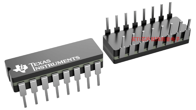
- 制造厂商:TI
- 产品类别:逻辑和电压转换
- 技术类目:触发器、锁存器和寄存器 - JK 触发器
- 功能描述:具有设置和复位端的双路正边沿触发式 J-K 触发器
- 点击这里打开及下载CD54ACT109的技术文档资料
- TI代理渠道,提供当日发货、严格的质量标准,满足您的目标价格

The ’ACT109 devices contain two independent J-K\ positive-edge-triggered flip-flops. A low level at the preset (PRE)\ or clear (CLR)\ inputs sets or resets the outputs, regardless of the levels of the other inputs. When PRE\ and CLR\ are inactive (high), data at the J and K\ inputs meeting the setup-time requirements are transferred to the outputs on the positive-going edge of the clock (CLK) pulse. Clock triggering occurs at a voltage level and is not directly related to the rise time of the clock pulse. Following the hold-time interval, data at the J and K\ inputs can be changed without affecting the levels at the outputs. These versatile flip-flops can perform as toggle flip-flops by grounding K\ and tying J high. They also can perform as D-type flip-flops if J and K\ are tied together.
- Inputs Are TTL-Voltage Compatible
- Speed of Bipolar F, AS, and S, With Significantly Reduced Power Consumption
- Balanced Propagation Delays
- ±24-mA Output Drive Current
- Fanout to 15 F Devices
- SCR-Latchup-Resistant CMOS Process and Circuit Design
- Exceeds 2-kV ESD Protection Per MIL-STD-883, Method 3015
- Number of channels (#)
- 2
- Technology Family
- ACT
- Supply voltage (Min) (V)
- 4.5
- Supply voltage (Max) (V)
- 5.5
- Input type
- TTL
- Output type
- Push-Pull
- Clock Frequency (MHz)
- 100
- ICC (Max) (uA)
- 80
- IOL (Max) (mA)
- -24
- IOH (Max) (mA)
- 24
- Features
- Balanced outputs, Positive edge triggered, High speed (tpd 10-50ns), Positive input clamp diode, Preset, Clear
CD54ACT109的完整型号有:CD54ACT109F3A,以下是这些产品的关键参数及官网采购报价:
CD54ACT109F3A,工作温度:-55 to 125,封装:CDIP (J)-16,包装数量MPQ:1个,MSL 等级/回流焊峰值温度:N/A for Pkg Type,引脚镀层/焊球材料:SNPB,TI官网CD54ACT109F3A的批量USD价格:4.675(1000+)

CD54ACT109F3A,工作温度:-55 to 125,封装:CDIP (J)-16,包装数量MPQ:1个,MSL 等级/回流焊峰值温度:N/A for Pkg Type,引脚镀层/焊球材料:SNPB,TI官网CD54ACT109F3A的批量USD价格:4.675(1000+)


