- 制造厂商:TI
- 产品类别:逻辑和电压转换
- 技术类目:专用逻辑 IC - 数字计时 IC
- 功能描述:数字锁相环系统
- 点击这里打开及下载CD74ACT297的技术文档资料
- TI代理渠道,提供当日发货、严格的质量标准,满足您的目标价格

The CD74ACT297 provides a simple, cost-effective solution to high-accuracy, digital, phase-locked-loop applications. This device contains all the necessary circuits, with the exception of the divide-by-N counter, to build first-order phase-locked loops as shown in Figure 1.
Both exclusive-OR phase detectors (XORPDs) and edge-controlled (ECPD) phase detectors are provided for maximum flexibility.
Proper partitioning of the loop function, with many of the building blocks external to the package, makes it easy for the designer to incorporate ripple cancellation or to cascade to higher-order phase-locked loops.
The length of the up/down K counter is digitally programmable according to the K-counter function table. With A, B, C, and D all low, the K counter is disabled. With A high and B, C, and D low, the K counter is only three stages long, which widens the bandwidth, or capture range, and shortens the lock time of the loop. When A, B, C, and D are programmed high, the K counter becomes 17 stages long, which narrows the bandwidth, or capture range, and lengthens the lock time. Real-time control of loop bandwidth by manipulating the A-through-D inputs can maximize the overall performance of the digital phase-locked loop.
This device performs the classic first-order phase-locked-loop function without using analog components. The accuracy of the digital phase-locked loop (DPLL) is not affected by VCC and temperature variations, but depends solely on accuracies of the K clock (K CLK), increment/decrement clock (I/D CLK), and loop propagation delays. The I/D clock frequency and the divide-by-N modulos determine the center frequency of the DPLL. The center frequency is defined by the relationship fc = I/D clock/2N (Hz).
- Speed of Bipolar FCT, AS, and S, With Significantly Reduced Power Consumption
- Digital Design Avoids Analog Compensation Errors
- Easily Cascadable for Higher-Order Loops
- Useful Frequency Range
- DC to 110 MHz Typical (K CLK)
- DC to 70 MHz Typical (I/D CLK)
- Dynamically Variable Bandwidth
- Very Narrow Bandwidth Attainable
- Power-On Reset
- Output Capability
- Standard: XORPD OUT, ECPD OUT
- Bus Driver: I/D OUT
- SCR Latch-Up-Resistant CMOS Process and Circuit Design
- Balanced Propagation Delays
- ESD Protection Exceeds 2000 V Per MIL-STD-883, Method 3015
- Technology Family
- ACT
- Bits (#)
- 1
- Supply voltage (Min) (V)
- 4.5
- Supply voltage (Max) (V)
- 5.5
- Input type
- TTL-Compatible CMOS
- Output type
- Push-Pull
- ICC (Max) (uA)
- 80
- IOL (Max) (mA)
- 24
- IOH (Max) (mA)
- -24
CD74ACT297的完整型号有:CD74ACT297M,以下是这些产品的关键参数及官网采购报价:
CD74ACT297M,工作温度:-55 to 125,封装:SOIC (D)-16,包装数量MPQ:40个,MSL 等级/回流焊峰值温度:Level-1-260C-UNLIM,引脚镀层/焊球材料:NIPDAU,TI官网CD74ACT297M的批量USD价格:1.304(1000+)

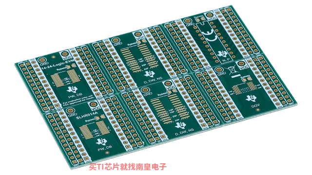
14-24-LOGIC-EVM 支持 14 到 24 引脚 PW、DB、D、DW、NS、DYY 和 DGV 封装的通用逻辑 EVM
该 EVM 设计用于支持采用 14 至 24 引脚 D、DW、DB、NS、PW、DYY 或 DGV 封装的任何逻辑器件。