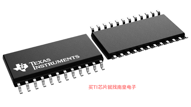
- 制造厂商:TI
- 产品类别:逻辑和电压转换
- 技术类目:触发器、锁存器和寄存器 - D 型锁存器
- 功能描述:具有三态输出的 BiCMOS FCT 接口逻辑 9 位同向透明锁存器
- 点击这里打开及下载CD74FCT843A的技术文档资料
- TI代理渠道,提供当日发货、严格的质量标准,满足您的目标价格

The CD74FCT843A is a 9-bit, bus-interface, D-type latch with 3-state outputs, designed specifically for driving highly capacitive or relatively low-impedance loads. It is particularly suitable for implementing buffer registers, I/O ports, bidirectional bus drivers, and working registers.
The device uses a small-geometry BiCMOS technology. The output stage is a combination of bipolar and CMOS transistors that limits the output high level to two diode drops below VCC. This resultant lowering of output swing (0 V to 3.7 V) reduces power-bus ringing [a source of electromagnetic interference (EMI)] and minimizes VCC bounce and ground bounce and their effects during simultaneous output switching. The output configuration also enhances switching speed and is capable of sinking 48 mA.
The CD74FCT843A outputs are transparent to the inputs when the latch-enable (LE) input is high. The latches are transparent D-type latches. When LE goes low, the data is latched. The output-enable (OE\) input controls the 3-state outputs. When OE\ is high, the outputs are in the high-impedance state. The latch operation is independent of the state of the output enable. This device, having preset (PRE\) and clear (CLR\), are ideal for parity-bus interfacing. When PRE\ is low, the outputs are high if OE\ is low. PRE\ overrides CLR\. When CLR\ is low, the outputs are low if OE\ is low. When CLR\ is high, data can be entered into the latch. The device provides noninverted outputs.
OE\ does not affect the internal operations of the latch. Previously stored data can be retained or new data can be entered while the outputs are in the high-impedance state.
The CD74FCT843A is characterized for operation from 0°C to 70°C.
- BiCMOS Technology With Low Quiescent Power
- Buffered Inputs
- Noninverted Outputs
- Input/Output Isolation From VCC
- Controlled Output Edge Rates
- 48-mA Output Sink Current
- Output Voltage Swing Limited to 3.7 V
- SCR Latch-Up-Resistant BiCMOS Process and Circuit Design
- Packaged in Plastic Small-Outline Package
- Number of channels (#)
- 9
- Technology Family
- FCT
- Supply voltage (Min) (V)
- 4.75
- Supply voltage (Max) (V)
- 5.25
- Input type
- TTL-Compatible CMOS
- Output type
- 3-State
- Clock Frequency (Max) (MHz)
- 70
- IOL (Max) (mA)
- 48
- IOH (Max) (mA)
- -15
- ICC (Max) (uA)
- 80
- Features
- Very high speed (tpd 5-10ns), Partial power down (Ioff), Flow-through pinout
CD74FCT843A的完整型号有:CD74FCT843AM,以下是这些产品的关键参数及官网采购报价:
CD74FCT843AM,工作温度:0 to 70,封装:SOIC (DW)-24,包装数量MPQ:25个,MSL 等级/回流焊峰值温度:Level-1-260C-UNLIM,引脚镀层/焊球材料:NIPDAU,TI官网CD74FCT843AM的批量USD价格:3.479(1000+)

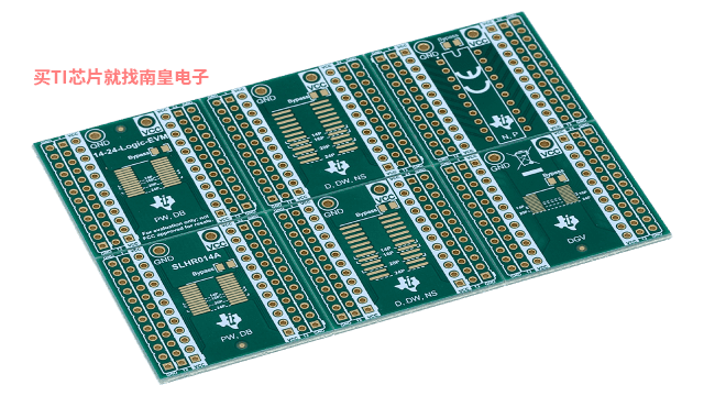
14-24-LOGIC-EVM ― 支持 14 到 24 引脚 PW、DB、D、DW、NS、DYY 和 DGV 封装的通用逻辑 EVM
该 EVM 设计用于支持采用 14 至 24 引脚 D、DW、DB、NS、PW、DYY 或 DGV 封装的任何逻辑器件。


