- 制造厂商:TI
- 产品类别:时钟和计时
- 技术类目:时钟缓冲器
- 功能描述:具有 I2C 控制接口的 1 线路至 18 线路时钟驱动器
- 点击这里打开及下载CDC318A的技术文档资料
- TI代理渠道,提供当日发货、严格的质量标准,满足您的目标价格

The CDC318A is a high-performance clock buffer designed to distribute high-speed clocks in PC applications. This device distributes one input (A) to 18 outputs (Y) with minimum skew for clock distribution. The CDC318A operates from a 3.3-V power supply. It is characterized for operation from 0°C to 70°C.
This device has been designed with consideration for optimized EMI performance. Depending on the application layout, damping resistors in series to the clock outputs (like proposed in the PC100 specification) may not be needed in most cases.
The device provides a standard mode (100K-bits/s) I2C serial interface for device control. The implementation is as a slave/receiver. The device address is specified in the I2C device address table. Both of the I2C inputs (SDATA and SCLOCK) are 5-V tolerant and provide integrated pullup resistors (typically 140 k ).
).
Three 8-bit I2C registers provide individual enable control for each of the outputs. All outputs default to enabled at powerup. Each output can be placed in a disabled mode with a low-level output when a low-level control bit is written to the control register. The registers are write only and must be accessed in sequential order (i.e., random access of the registers is not supported).
The CDC318A provides 3-state outputs for testing and debugging purposes. The outputs can be placed in a high-impedance state via the output-enable (OE) input. When OE is high, all outputs are in the operational state. When OE is low, the outputs are placed in a high-impedance state. OE provides an integrated pullup resistor.
- High-Speed, Low-Skew 1-to-18 Clock Buffer for Synchronous DRAM (SDRAM) Clock Buffering Applications
- Output Skew, tsk(o), Less Than 250 ps
- Pulse Skew, tsk(p), Less Than 500 ps
- Supports up to Four Unbuffered SDRAM Dual Inline Memory Modules (DIMMs)
- I2C Serial Interface Provides Individual Enable Control for Each Output
- Operates at 3.3 V
- Distributed VCC and Ground Pins Reduce Switching Noise
- 100-MHz Operation
- ESD Protection Exceeds 2000 V Per MIL-STD-883, Method 3015
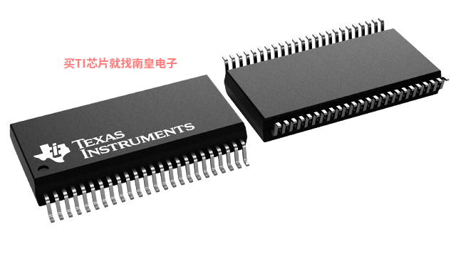
- Packaged in 48-Pin Shrink Small Outline (DL) Package
- Function
- Single-ended
- Output frequency (Max) (MHz)
- 100
- Number of outputs
- 18
- Output supply voltage (V)
- 3.3
- Core supply voltage (V)
- 3.3
- Output skew (ps)
- 250
- Features
- I2C interface
- Operating temperature range (C)
- 0 to 70
- Rating
- Catalog
- Output type
- LVTTL
- Input type
- LVTTL
CDC318A的完整型号有:CDC318ADL、CDC318ADLR,以下是这些产品的关键参数及官网采购报价:
CDC318ADL,工作温度:0 to 70,封装:SSOP (DL)-48,包装数量MPQ:25个,MSL 等级/回流焊峰值温度:Level-2-260C-1 YEAR,引脚镀层/焊球材料:NIPDAU,TI官网CDC318ADL的批量USD价格:4.267(1000+)
CDC318ADLR,工作温度:0 to 70,封装:SSOP (DL)-48,包装数量MPQ:1000个,MSL 等级/回流焊峰值温度:Level-2-260C-1 YEAR,引脚镀层/焊球材料:NIPDAU,TI官网CDC318ADLR的批量USD价格:3.635(1000+)

CDC318A IBIS Model
PSpice for TI 可提供帮助评估模拟电路功能的设计和仿真环境。此功能齐全的设计和仿真套件使用 Cadence 的模拟分析引擎。PSpice for TI 可免费使用,包括业内超大的模型库之一,涵盖我们的模拟和电源产品系列以及精选的模拟行为模型。借助?PSpice for TI 的设计和仿真环境及其内置的模型库,您可对复杂的混合信号设计进行仿真。创建完整的终端设备设计和原型解决方案,然后再进行布局和制造,可缩短产品上市时间并降低开发成本。
在?PSpice for TI 设计和仿真工具中,您可以搜索 TI (...)