- 制造厂商:TI
- 产品类别:时钟和计时
- 技术类目:时钟缓冲器
- 功能描述:具有 LDO 的四路正弦波时钟缓冲器
- 点击这里打开及下载CDC3S04的技术文档资料
- TI代理渠道,提供当日发货、严格的质量标准,满足您的目标价格

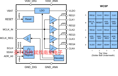
The CDC3S04 is a four-channel low-power low-jitter sine-wave clock buffer. It can be used to buffer a single master clock to multiple peripherals. The four sine-wave outputs (CLK1–CLK4) are designed for minimal channel-to-channel skew and ultralow additive output jitter.
Each output has its own clock request inputs which enables the dedicated clock output. These clock requests are active-high (can also be changed to be active-low via I2C), and an output signal is generated that can be sent back to the master clock to request the clock (MCLK_REQ). MCKL_REQ is an open-source output and supports the wired-OR function (default mode). It needs an external pulldown resistor. MCKL_REQ can be changed to wired-AND or push-pull functionality via I2C.
The CDC3S04 also provides an I2C interface (Hs-mode) that can be used to enable or disable the outputs, select the polarity of the REQ inputs, and allow control of internal decoding.
The CDC3S04 features an on-chip high-performance LDO that accepts voltages from 2.3 V to 5.5 V and outputs a 1.8-V supply. This 1.8-V supply can be used to power an external 1.8-V TCXO. It can be enabled or disabled for power saving at the TCXO.
A low signal at the RESET input switches the outputs CLK1 and CLK4 into the default state. In this configuration, CLK1 and CLK4 are ON (see ); the remaining device function is not affected. Also, the RESET input provides a glitch filter which rejects spikes of typical 300 ns on the RESET line to preserve false reset. A complete device reset to the default condition can be initiated by a power-up cycle of VDD_DIG.
The CDC3S04 operates from two 1.8-V supplies. There is a core supply (VDD_DIG/GND_DIG) for the core logic and a low-noise analog supply (VDD_ANA/GND_ANA) for the sine-wave outputs. The CDC3S04 is designed for sequence-less power up. Both supply voltages may be applied in any order.
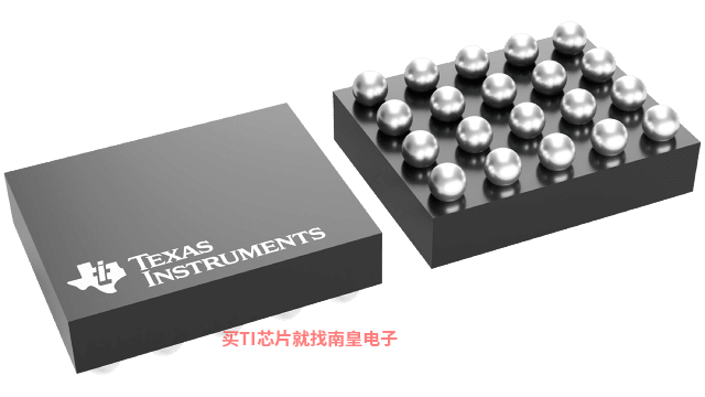
The CDC3S04 is offered in a 0.4-mm pitch WCSP package (1.6 mm × 2 mm) and is optimized for low standby current (0.5 µA). It is characterized for operation from –40°C to 85°C.
- 1:4 Low-Jitter Clock Buffer
- Single-Ended Sine-Wave Clock Input and Outputs
- Ultralow Phase Noise and Standby Current
- Individual Clock Request Inputs for Each Output
- On-Chip Low-Dropout Output (LDO) for Low-Noise TCXO Supply
- Serial I2C Interface (Compatible With High-Speed Mode, 3.4 Mbit/s)
- 1.8-V Device Power Supply
- Wide Temperature Range, –40°C to 85°C
- ESD Protection: 2 KV HBM, 750 V CDM, and 100 V MM
- Small 20-Pin Chip-Scale Package: 0.4-mm Pitch WCSP (1.6 mm × 2 mm)
- Function
- Single-ended
- Additive RMS jitter (Typ) (fs)
- 300
- Output frequency (Max) (MHz)
- 52
- Number of outputs
- 4
- Output supply voltage (V)
- 1.8
- Core supply voltage (V)
- 1.8
- Output skew (ps)
- 50
- Features
- SINE wave
- Operating temperature range (C)
- -40 to 85
- Rating
- Catalog
- Output type
- SINE
- Input type
- SINE
CDC3S04的完整型号有:CDC3S04YFFR,以下是这些产品的关键参数及官网采购报价:
CDC3S04YFFR,工作温度:-40 to 85,封装:DSBGA (YFF)-20,包装数量MPQ:3000个,MSL 等级/回流焊峰值温度:Level-1-260C-UNLIM,引脚镀层/焊球材料:SNAGCU,TI官网CDC3S04YFFR的批量USD价格:1.346(1000+)

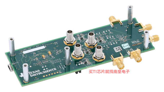
CDC3S04EVM — CDC3S04 评估模块
CDC3S04 是一款四通道、低功耗、正弦波时钟缓冲器。它可用于将一个单个的主时钟缓冲为多个外设。四个正弦波输出 (CLK1–CLK4) 针对最小化的通道到通道偏移和超低的附加输出抖动而设计。每个输出都具有其自己的启用了专用时钟输出的时钟请求输入。这些时钟请求为高电平有效(也可通过 I2C 更改为低电平有效),并生成一个输出信号,该输出信号可以发送回主时钟以请求时钟(MCLK_REQ)。MCKL_REQ 为开放源码输出,默认模式下支持线或功能。它需要一个外部下拉电阻。MCKL_REQ 可通过 I2C 更改为线与或推挽功能。此评估模块 (EVM) 旨在演示 CDC3S04 (...)CDC3S04 IBIS Model (Rev. A)
PSpice for TI 可提供帮助评估模拟电路功能的设计和仿真环境。此功能齐全的设计和仿真套件使用 Cadence 的模拟分析引擎。PSpice for TI 可免费使用,包括业内超大的模型库之一,涵盖我们的模拟和电源产品系列以及精选的模拟行为模型。借助?PSpice for TI 的设计和仿真环境及其内置的模型库,您可对复杂的混合信号设计进行仿真。创建完整的终端设备设计和原型解决方案,然后再进行布局和制造,可缩短产品上市时间并降低开发成本。
在?PSpice for TI 设计和仿真工具中,您可以搜索 TI (...)
CLOCK-TREE-ARCHITECT — 时钟树架构编程软件
时钟树架构是一款时钟树综合工具,可根据您的系统要求生成时钟树解决方案,从而帮助您简化设计流程。该工具从庞大的时钟产品数据库中提取数据,然后生成系统级多芯片时钟解决方案。