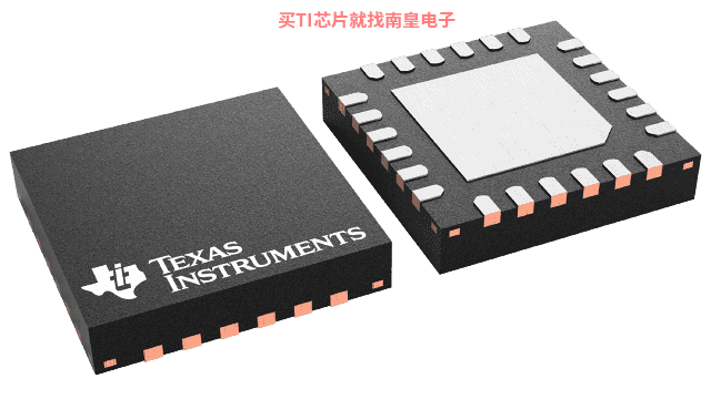
- 制造厂商:TI
- 产品类别:时钟和计时
- 技术类目:时钟发生器
- 功能描述:106.25MHz 全集成式固定频率低抖动晶振时钟发生器
- 点击这里打开及下载CDC421A106的技术文档资料
- TI代理渠道,提供当日发货、严格的质量标准,满足您的目标价格

The CDC421Axxx is a high-performance, low-phase-noise clock generator. It has an integrated low-noise, LC-based voltage-controlled oscillator (VCO) that operates within the 1.75 GHz to 2.35 GHz frequency range. It has an integrated crystal oscillator that operates in conjunction with an external AT-cut crystal to produce a stable frequency reference for a phase-locked loop (PLL)-based frequency synthesizer. The output frequency (fOUT) is proportional to the frequency of the input crystal (fXTAL).
The device operates in 3.3-V supply environment and is characterized for operation from -40°C to +85°C. The CDC421Axxx is available in a QFN-24 4-mm × 4-mm package.
The CDC421Axxx differs from the CDC421xxx in the following ways:
- Device Startup
The CDC421Axxx has an improved startup circuit to enable correct operation for all power-supply ramp times.
- Single 3.3-V Supply
- High-Performance Clock Generator, Incorporating Crystal Oscillator Circuitry with Integrated Frequency Synthesizer
- Low Output Jitter: As low as 380 fs (RMS integrated between 10 kHz to 20 MHz)
- Low Phase Noise at 312.5 MHz:
- Less than -120 dBc/Hz at 10 kHz and -147 dBc/Hz at 10-MHz offset from carrier
- Supports Crystal or LVCMOS Input Frequencies at 31.25 MHz, 33.33 MHz, and 35.42 MHz
- Output Frequencies: 100 MHz, 106.25 MHz, 125 MHz, 156.25 MHz, 212.5 MHz, 250 MHz, and 312.5 MHz
- Differential Low-Voltage Positive Emitter Coupled Logic (LVPECL) Outputs
- Fully-Integrated Voltage-Controlled Oscillator (VCO): Runs from 1.75 GHz to 2.35 GHz
- Typical Power Consumption: 300 mW
- Chip Enable Control Pin
- Available in 4-mm × 4-mm QFN-24 Package
- ESD Protection Exceeds 2 kV (HBM)
- Industrial Temperature Range: -40°C to +85°C
- APPLICATIONS
- Low-Cost, Low-Jitter Frequency Multiplier
All trademarks are the property of their respective owners.
- Function
- Clock generator
- Number of outputs
- 1
- Output frequency (Max) (MHz)
- 106.25
- Core supply voltage (V)
- 3.3
- Output supply voltage (V)
- 3.3
- Input type
- LVCMOS
- Output type
- LVPECL
- Operating temperature range (C)
- -40 to 85
- Features
- Signal 3.3-V supply, Chip-enable control pin
- Rating
- Catalog
CDC421A106的完整型号有:CDC421A106RGER、CDC421A106RGET,以下是这些产品的关键参数及官网采购报价:
CDC421A106RGER,工作温度:-40 to 85,封装:VQFN (RGE)-24,包装数量MPQ:3000个,MSL 等级/回流焊峰值温度:Level-2-260C-1 YEAR,引脚镀层/焊球材料:NIPDAU,TI官网CDC421A106RGER的批量USD价格:6.468(1000+)
CDC421A106RGET,工作温度:-40 to 85,封装:VQFN (RGE)-24,包装数量MPQ:250个,MSL 等级/回流焊峰值温度:Level-2-260C-1 YEAR,引脚镀层/焊球材料:NIPDAU,TI官网CDC421A106RGET的批量USD价格:7.762(1000+)

PSPICE-FOR-TI ― 适用于 TI 设计和模拟工具的 PSpice
PSpice for TI 可提供帮助评估模拟电路功能的设计和仿真环境。此功能齐全的设计和仿真套件使用 Cadence 的模拟分析引擎。PSpice for TI 可免费使用,包括业内超大的模型库之一,涵盖我们的模拟和电源产品系列以及精选的模拟行为模型。借助?PSpice for TI 的设计和仿真环境及其内置的模型库,您可对复杂的混合信号设计进行仿真。创建完整的终端设备设计和原型解决方案,然后再进行布局和制造,可缩短产品上市时间并降低开发成本。
在?PSpice for TI 设计和仿真工具中,您可以搜索 TI (...)


