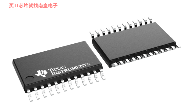
- 制造厂商:TI
- 产品类别:时钟和计时
- 技术类目:时钟缓冲器
- 功能描述:3.3V 相位锁定环路时钟驱动器
- 点击这里打开及下载CDC509的技术文档资料
- TI代理渠道,提供当日发货、严格的质量标准,满足您的目标价格

The CDC509 is a high-performance, low-skew, low-jitter, phase-lock loop (PLL) clock driver. It uses a PLL to precisely align, in both frequency and phase, the feedback (FBOUT) output to the clock (CLK) input signal. It is specifically designed for use with synchronous DRAMs. The CDC509 operates at 3.3-V VCC and is designed to drive up to five clock loads per output.
One bank of five outputs and one bank of four outputs provide nine low-skew, low-jitter copies of CLK. Output signal duty cycles are adjusted to 50 percent, independent of the duty cycle at CLK. Each bank of outputs can be enabled or disabled separately via the control (1G and 2G) inputs. When the G inputs are high, the outputs switch in phase and frequency with CLK; when the G inputs are low, the outputs are disabled to the logic-low state.
Unlike many products containing PLLs, the CDC509 does not require external RC networks. The loop filter for the PLL is included on-chip, minimizing component count, board space, and cost.
Because it is based on PLL circuitry, the CDC509 requires a stabilization time to achieve phase lock of the feedback signal to the reference signal. This stabilization time is required, following power up and application of a fixed-frequency, fixed-phase signal at CLK, as well as following any changes to the PLL reference or feedback signals. The PLL can be bypassed for test purposes by strapping AVCC to ground.
The CDC509 is characterized for operation from 0°C to 70°C.
- Use CDCVF2509A as a Replacement for this Device
- Phase-Lock Loop Clock Distribution for Synchronous DRAM Applications
- Distributes One Clock Input to One Bank of Five and One Bank of Four Outputs
- Separate Output Enable for Each Output Bank
- External Feedback (FBIN) Pin Is Used to Synchronize the Outputs to the Clock Input
- No External RC Network Required
- Operates at 3.3-V VCC
- Packaged in Plastic 24-Pin Thin Shrink Small-Outline Package
- Function
- Zero-delay
- Additive RMS jitter (Typ) (fs)
- 200
- Output frequency (Max) (MHz)
- 125
- Number of outputs
- 9
- Output supply voltage (V)
- 3.3
- Core supply voltage (V)
- 3.3
- Output skew (ps)
- 200
- Operating temperature range (C)
- 0 to 70
- Rating
- Catalog
- Output type
- TTL
- Input type
- TTL
CDC509的完整型号有:CDC509PWR,以下是这些产品的关键参数及官网采购报价:
CDC509PWR,工作温度:0 to 70,封装:TSSOP (PW)-24,包装数量MPQ:2000个,MSL 等级/回流焊峰值温度:Level-1-260C-UNLIM,引脚镀层/焊球材料:NIPDAU,TI官网CDC509PWR的批量USD价格:8.898(1000+)

CDC509 IBIS Model
PSpice for TI 可提供帮助评估模拟电路功能的设计和仿真环境。此功能齐全的设计和仿真套件使用 Cadence 的模拟分析引擎。PSpice for TI 可免费使用,包括业内超大的模型库之一,涵盖我们的模拟和电源产品系列以及精选的模拟行为模型。借助?PSpice for TI 的设计和仿真环境及其内置的模型库,您可对复杂的混合信号设计进行仿真。创建完整的终端设备设计和原型解决方案,然后再进行布局和制造,可缩短产品上市时间并降低开发成本。
在?PSpice for TI 设计和仿真工具中,您可以搜索 TI (...)


