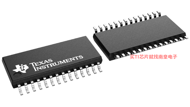
- 制造厂商:TI
- 产品类别:时钟和计时
- 技术类目:时钟缓冲器
- 功能描述:Rambus XDR 时钟发生器
- 点击这里打开及下载CDCD5704的技术文档资料
- TI代理渠道,提供当日发货、严格的质量标准,满足您的目标价格

The CDCD5704 clock generator provides the necessary clock signals to support an XDR memory subsystem and Redwood logic interface using a reference clock input with or without spread-spectrum modulation. Contained in a 28-pin TSSOP package that includes four differential clock outputs, the CDCD5704 provides an off-the-shelf solution for a broad range of high-performance interface applications.
The block diagram shows the major components of the CDCD5704, which include a phase-locked loop, a bypass multiplexer, and four differential output buffers (CLK0 to CLK3). All four outputs can be disabled by a logical low at the input of the EN pin. An output is enabled when EN is high and a value of 1 is in its serial interface register (RegA-RegD).
The PLL receives a reference clock input signal, REFCLK, and outputs a clock signal at a frequency equal to the input frequency times the multiplication factor. The PLL output clock signal is fed to the differential output buffers to drive the enabled clocks. Disabled outputs are set to high impedance.
The bypass mode routes the input clock REFCLK to the differential output buffers, bypassing the PLL.
To ensure that the CDCD5704 clock generator always performs correctly, the device switches off the PLL and the outputs are in the high-impedance state, once the clock input is below 10 MHz. If the supply voltage VDD is less than VPUC, all logic gates are reset, the PLL is powered down, and the outputs are in the high-impedance state. Therefore, the device only starts its operation if these minimum requirements are met.
Because the CDCD5704 is based on PLL circuitry, it requires a stabilization time to achieve phase-lock of the PLL. With use of an external reference clock, this signal must be fixed-frequency and fixed-phase prior to the start of stabilization time.
The device operates from a single 2.5-V supply voltage. The CDCD5704 device is characterized for operation from 0°C to 70°C.
- High-Speed Clock Support: 300-MHz-667-MHz Clock Source for XDR Memory Subsystems and Redwood Logic Interface
- Quad (Open-Drain) Differential Output Drivers
- Spread-Spectrum Compatible Clock Input Can Be Distributed to Minimize EMI
- Differential or Single-Ended Reference Clock Input of 100 MHz or 133 MHz
- Serial Interface Features: Programmable Frequency Multiplier, Select Any One to Four Outputs and Mode of Operation
- Supports Frequency Multiplication Factors of: ×3, ×4, ×5, ×6, ×8, ×9/2, ×15/2, ×15/4
- All PLL Loop Filter Components Are Integrated
- Low |Cycle-to-Cycle| of 1-6 Cycle Jitter:
- 40 ps: 300-635 MHz
- 30 ps: 636-667 MHz
- PLLs Are Powered Down if No Valid REF Clock (<10 MHz) Is Detected or VDD Is Below 1.6 V
- Operates From Single 2.5-V Supply (±0.125 V)
- Packaged in TSSOP-28
- Commercial Temperature Range 0°C to 70°C
- APPLICATIONS
- XDR Memory Subsystem and Redwood Logic Interface
Rambus, XDR are trademarks of Rambus Inc. All other trademarks are the property of their respective owners.
- Function
- Memory interface
- Additive RMS jitter (Typ) (fs)
- 30
- Output frequency (Max) (MHz)
- 667
- Number of outputs
- 4
- Output supply voltage (V)
- 2.5
- Core supply voltage (V)
- 2.5
- Output skew (ps)
- 15
- Features
- Spread spectrum clocking (SSC)
- Operating temperature range (C)
- 0 to 70
- Rating
- Catalog
- Output type
- TTL
- Input type
- TTL
CDCD5704的完整型号有:CDCD5704PW、CDCD5704PWR,以下是这些产品的关键参数及官网采购报价:
CDCD5704PW,工作温度:0 to 70,封装:TSSOP (PW)-28,包装数量MPQ:50个,MSL 等级/回流焊峰值温度:Level-1-260C-UNLIM,引脚镀层/焊球材料:NIPDAU,TI官网CDCD5704PW的批量USD价格:3.115(1000+)
CDCD5704PWR,工作温度:0 to 70,封装:TSSOP (PW)-28,包装数量MPQ:2000个,MSL 等级/回流焊峰值温度:Level-1-260C-UNLIM,引脚镀层/焊球材料:NIPDAU,TI官网CDCD5704PWR的批量USD价格:2.596(1000+)

CDCD5704 IBIS model
PSpice for TI 可提供帮助评估模拟电路功能的设计和仿真环境。此功能齐全的设计和仿真套件使用 Cadence 的模拟分析引擎。PSpice for TI 可免费使用,包括业内超大的模型库之一,涵盖我们的模拟和电源产品系列以及精选的模拟行为模型。借助?PSpice for TI 的设计和仿真环境及其内置的模型库,您可对复杂的混合信号设计进行仿真。创建完整的终端设备设计和原型解决方案,然后再进行布局和制造,可缩短产品上市时间并降低开发成本。
在?PSpice for TI 设计和仿真工具中,您可以搜索 TI (...)


