- ���쳧�̣�TI
- ��Ʒ���ʱ�Ӻͼ�ʱ
- ������Ŀ��ʱ�ӻ�����
- �������������з�Ƶ���� 5/10 ·���ʱ�ӻ�����
- ������������CDCE18005�ļ����ĵ�����
- TI�����������ṩ���շ������ϸ������������������Ŀ��۸�

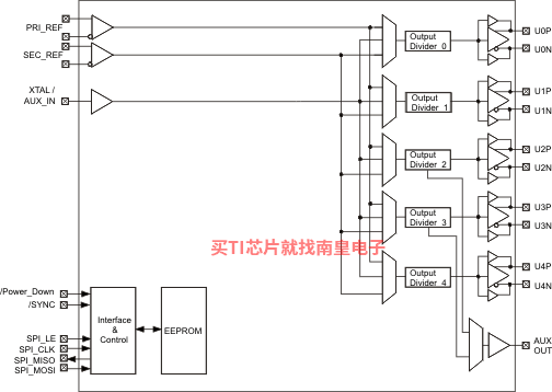
The CDCE18005 is a high performance clock distributor featuring a high degree of configurability via a SPI interface, and programmable start up modes determined by on-chip EEPROM. Specifically tailored for buffering clocks for data converters and high-speed digital signals, the CDCE18005 achieves low additive jitter in the 50 fs RMS(1) range. The clock distribution block includes five individually programmable outputs that can be configured to provide different combinations of output formats (LVPECL, LVDS, LVCMOS). Each output can also be programmed to a unique output frequency (up to 1.5 GHz(2)
- Universal Input Buffers That Accept LVPECL, LVDS, or LVCMOS Level Signaling
- Fully Configurable Outputs Including Frequency, Output Format, and Output Skew
- Output Multiplexer That Serves as a Clock Switch Between the Three Reference Inputs and the Outputs
- Clock Generation Via AT-Cut Crystal
- Integrated EEPROM Determines Device Configuration at Power-up
- Low Additive Jitter Performance
- Universal Output Blocks Support up to 5 Differential, 10 Single-ended, or Combinations of Differential or Single-ended:
- Low Additive Jitter
- Output Frequency up to 1.5 GHz
- LVPECL, LVDS, LVCMOS, and Special High Output Swing Modes
- Independent Output Dividers Support Divide Ratios from 1�C80
- Independent limited Coarse Skew Control on all Outputs
- Flexible Inputs:
- Two Universal Differential Inputs Accept Frequencies up to 1500 MHz (LVPECL), 800 MHz (LVDS), or 250 MHz (LVCMOS).
- One Auxiliary Input Accepts Crystal. Auxiliary Input Accepts Crystals in the Range of 2 MHz�C42 MHz
- Clock Generator Mode Using Crystal Input.
- Typical Power Consumption 1W at 3.3V
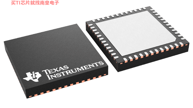
- Offered in QFN-48 Package
- ESD Protection Exceeds 2kV HBM
- Industrial Temperature Range �C40��C to 85��C
- Function
- Differential
- Additive RMS jitter (Typ) (fs)
- 200
- Output frequency (Max) (MHz)
- 1500
- Number of outputs
- 5
- Output supply voltage (V)
- 3.3
- Core supply voltage (V)
- 3.3
- Output skew (ps)
- 25
- Features
- Integrated EEPROM
- Operating temperature range (C)
- -40 to 85
- Rating
- Catalog
- Output type
- LVPECL
- Input type
- LVPECL
CDCE18005�������ͺ��У�CDCE18005RGZR��CDCE18005RGZT����������Щ��Ʒ�Ĺؼ������������ɹ����ۣ�
CDCE18005RGZR�������¶ȣ�-40 to 85����װ��VQFN (RGZ)-48����װ����MPQ��2500����MSL �ȼ�/��������ֵ�¶ȣ�Level-3-260C-168 HR�����ŶƲ�/������ϣ�NIPDAUAG��TI����CDCE18005RGZR������USD�۸�6.098��1000+��
CDCE18005RGZT�������¶ȣ�-40 to 85����װ��VQFN (RGZ)-48����װ����MPQ��250����MSL �ȼ�/��������ֵ�¶ȣ�Level-3-260C-168 HR�����ŶƲ�/������ϣ�NIPDAUAG��TI����CDCE18005RGZT������USD�۸�7.207��1000+��

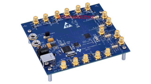
CDCE18005EVM �� CDCE18005EVM ����ģ��
CDCE18005 �Ǹ�����ʱ�ӷ������ͷ������������и߶ȿ������ԣ�ͨ�� SPI �ӿڽ������ã�����Ƭ�� EEPROM ȷ���Ŀɱ������ģʽ��רΪ����ת�������������źŵĻ���ʱ�Ӷ���ƣ�CDCE18005 ʵ���� 50 fs ��Χ���ڵĵ��Ӷ�����ʱ�ӷ������� 5 �������Ŀɱ����������ǿ������ó��ṩ��ͬ�������ʽ��ϣ�LVPECL��LVDS��LVCMOS����Ҳ����ͨ���ɱ���ӳٿ齫ÿ��������Ϊ���ص����Ƶ�ʣ��ߴ� 1.5GHzGHz����ƫ�ƹ�ϵ�����������������õ���ģʽ������ LVCMOS���������ã��� CDCE18005 ��֧�ֶ�� 10 ·�����ÿ�����������ѡ�� 3 (...)CDCE18005 EVM Control Software installer (Rev. A)
PSpice for TI ���ṩ��������ģ���·���ܵ���ƺͷ��滷�����˹�����ȫ����ƺͷ�����ʹ�� Cadence ��ģ��������档PSpice for TI �����ʹ�ã�����ҵ�ڳ����ģ�Ϳ�֮һ���������ǵ�ģ��͵�Դ��Ʒϵ���Լ���ѡ��ģ����Ϊģ�͡�����?PSpice for TI ����ƺͷ��滷���������õ�ģ�Ϳ⣬���ɶԸ��ӵĻ���ź���ƽ��з��档�����������ն��豸��ƺ�ԭ�ͽ��������Ȼ���ٽ��в��ֺ����죬�����̲�Ʒ����ʱ�䲢���Ϳ����ɱ���
��?PSpice for TI ��ƺͷ��湤���У����������� TI (...)