- ���쳧�̣�TI
- ��Ʒ���ʱ�Ӻͼ�ʱ
- ������Ŀ��ʱ�ӷ�����
- �������������м���˫· VCO �� 4 ·���ʱ�ӷ�����/����������
- ������������CDCE62002�ļ����ĵ�����
- TI�����������ṩ���շ������ϸ������������������Ŀ��۸�

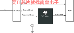
The CDCE62002 device is a high-performance clock generator featuring low output jitter, a high degree of configurability through a SPI interface, and programmable start-up modes determined by on-chip EEPROM. Specifically tailored for clocking data converters and high-speed digital signals, the CDCE62002 achieves jitter performance under 0.5 ps RMS(1).
It incorporates a synthesizer block with partially integrated loop filter, a clock distribution block including programmable output formats, and an input block featuring an innovative smart multiplexer. The clock distribution block includes two individually programmable outputs that can be configured to provide different combinations of output formats (LVPECL, LVDS, LVCMOS). Each output can also be programmed to a unique output frequency (ranging from 10.94 MHz to 1.175 GHz(2)). If Both outputs are configured in single-ended mode (such as LVCMOS), the CDCE62002 supports up to four outputs. The input block includes one universal differential inputs which support frequencies up to 500 MHz and an auxiliary input that can be configured to connect to an external AT-Cut crystal through an onboard oscillator block. The smart input multiplexer has two modes of operation, manual and automatic. In manual mode, the user selects the synthesizer reference through the SPI interface. In automatic mode, the input multiplexer will automatically select between the highest priority input clock available.
(1) 10-kHz to 20-MHz integration bandwidth.
(2) Frequency range depends on operational mode and output format selected.
- Frequency Synthesizer With PLL/VCO and Partially Integrated Loop Filter
- Fully Configurable Outputs Including Frequency and Output Format
- Smart Input Multiplexer Automatically Switches Between One of Two Reference Inputs
- Multiple Operational Modes Include Clock Generation Through Crystal, SERDES Start-Up Mode, Jitter Cleaning, and Oscillator Based Holdover Mode
- Integrated EEPROM Determines Device Configuration at Power Up
- Excellent Jitter Performance
- Integrated Frequency Synthesizer Including PLL, Multiple VCOs, and Loop Filter:
- Full Programmability Facilitates Phase Noise Performance Optimization Enabling Jitter Cleaner Mode
- Programmable Charge Pump Gain and Loop Filter Settings
- Unique Dual-VCO Architecture Supports a Wide Tuning Range 1.750 GHz to 2.356 GHz.
- Universal Output Blocks Support Up to 2 Differential, 4 Single-Ended, or Combinations of Differential or Single-Ended:
- 0.5 ps RMS (10 kHz to 20 MHz) Output Jitter Performance
- Low Output Phase Noise: �C130 dBc/Hz at 1?MHz Offset, Fc = 491.52 MHz
- Output Frequency Ranges From 10.94 MHz to 1.175 GHz in Synthesizer Mode
- LVPECL, LVDS, and LVCMOS
- Independent Output Dividers Support Divide Ratios for 1, 2, 3, 4, 5, 8, 10, 12, 16, 20, 24, and 32
- Flexible Inputs With Innovative Smart Multiplexer:
- Two Universal Differential Inputs Accept Frequencies from 1 MHz up to 500 MHz (LVPECL), 500 MHz (LVDS), or 250 MHz (LVCMOS)
- One Auxiliary Input Accepts Crystals in the Range of 2 MHz to 42 MHz
- Clock Generator Mode Using Crystal Input
- Smart Input Multiplexer Can be Configured to Automatically Switch Between Highest Priority Clock Source Available Allowing for Fail-Safe Operation
- Typical Power Consumption 750 mW at 3.3 V
- Integrated EEPROM Stores Default Settings; Therefore, the Device Can Power Up in a Known, Predefined State
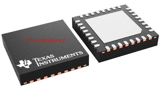
- Offered in QFN-32 Package
- ESD Protection Exceeds 2000 V HBM
- Industrial Temperature Range: �C40��C to +85��C
- APPLICATIONS
- Data Converter and Data Aggregation Clocking
- Wireless Infrastructure
- Switches and Routers
- Medical Electronics
- Military and Aerospace
- Industrial
- Clock Generation and Jitter Cleaning
All other trademarks are the property of their respective owners
- Function
- Clock generator
- Number of outputs
- 2
- Output frequency (Max) (MHz)
- 1175
- Core supply voltage (V)
- 3.3
- Output supply voltage (V)
- 3.3
- Input type
- LVPECL
- Output type
- LVPECL
- Operating temperature range (C)
- -40 to 85
- Features
- Design tool available, Integrated EEPROM, Serial interface
- Rating
- Catalog
CDCE62002�������ͺ��У�CDCE62002RHBR��CDCE62002RHBT����������Щ��Ʒ�Ĺؼ������������ɹ����ۣ�
CDCE62002RHBR�������¶ȣ�-40 to 85����װ��VQFN (RHB)-32����װ����MPQ��3000����MSL �ȼ�/��������ֵ�¶ȣ�Level-2-260C-1 YEAR�����ŶƲ�/������ϣ�NIPDAU��TI����CDCE62002RHBR������USD�۸�2.86��1000+��
CDCE62002RHBT�������¶ȣ�-40 to 85����װ��VQFN (RHB)-32����װ����MPQ��250����MSL �ȼ�/��������ֵ�¶ȣ�Level-2-260C-1 YEAR�����ŶƲ�/������ϣ�NIPDAU��TI����CDCE62002RHBT������USD�۸�3.432��1000+��

CDCE62002EVM �� CDCE62002 Evaluation Module
CDCE62002EVM ������ CDCE62002 ������ģ�顣CDCE62002 �Ǹ�����ʱ�ӷ������������е�����������߶ȿ������ԣ�ͨ�� SPI �ӿڽ������ã�����Ƭ�� EEPROM ȷ���Ŀɱ������ģʽ��CDCE62002 ʵ���˵��� 0.5ps RMS �Ķ������ܡ�
CDCE62002RHB_EVM GUI (Rev. B)
PSpice for TI ���ṩ��������ģ���·���ܵ���ƺͷ��滷�����˹�����ȫ����ƺͷ�����ʹ�� Cadence ��ģ��������档PSpice for TI �����ʹ�ã�����ҵ�ڳ����ģ�Ϳ�֮һ���������ǵ�ģ��͵�Դ��Ʒϵ���Լ���ѡ��ģ����Ϊģ�͡�����?PSpice for TI ����ƺͷ��滷���������õ�ģ�Ϳ⣬���ɶԸ��ӵĻ���ź���ƽ��з��档�����������ն��豸��ƺ�ԭ�ͽ��������Ȼ���ٽ��в��ֺ����죬�����̲�Ʒ����ʱ�䲢���Ϳ����ɱ���
��?PSpice for TI ��ƺͷ��湤���У����������� TI (...)