- 制造厂商:TI
- 产品类别:时钟和计时
- 技术类目:时钟发生器
- 功能描述:Ultra-low power clock generator with one PLL, four differential output
- 点击这里打开及下载CDCE6214的技术文档资料
- TI代理渠道,提供当日发货、严格的质量标准,满足您的目标价格

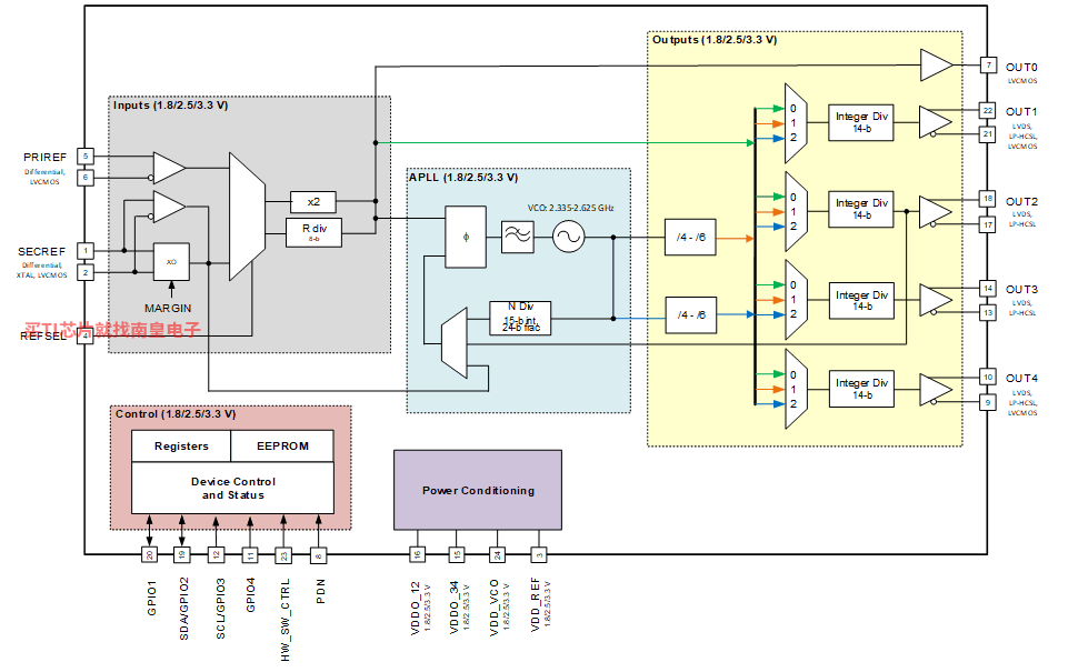
The CDCE6214 is a four-channel, ultra-low power, medium grade jitter, clock generator that can generate five independent clock outputs selectable between various modes of drivers. The input source could be a single-ended or differential input clock source, or a crystal. The CDCE6214 features a frac-N PLL to synthesize unrelated base frequency from any input frequency. The CDCE6214 can be configured through the I2C interface. In the absence of the serial interface, the GPIO pins can be used in Pin Mode to configure the product into distinctive configurations.
On-chip EEPROM can be used to change the configuration, which is pre-selectable through the pins. The device provides frequency margining options with glitch-free operation to support system design verification tests (DVT) and Ethernet Audio-Video Bridging (eAVB). Fine frequency margining is available on any output channel by steering the fractional feedback divider in DCO mode.
Internal power conditioning provides excellent power supply ripple rejection (PSRR), reducing the cost and complexity of the power delivery network. The analog and digital core blocks operate from either a 1.8-V, 2.5-V, or 3.3-V ±5% supply, and output blocks operate from a 1.8-V, 2.5-V, or 3.3-V ±5% supply.
The CDCE6214 enables high-performance clock trees from a single reference at ultra-low power with a small footprint. The factory- and user-programmable EEPROM features make the CDCE6214 an easy-to-use, instant-on clocking device with a low power consumption.
- Configurable high performance, low-power, frac-N PLL with RMS jitter with spurs (12 kHz 20 MHz, Fout > 100 MHz) as:
- Integer mode:
- Differential output: 350 fs typical, 600 fs maximum
- LVCMOS output: 1.05 ps typical, 1.5 ps maximum
- Fractional mode:
- Differential output: 1.7 ps typical, 2.1 ps maximum
- LVCMOS output: 2.0 ps typical, 4.0 ps maximum
- Integer mode:
- Supports PCIe Gen1/2/3/4 with SSC and Gen 1/2/3/4/5 without SSC
- 2.335-GHz to 2.625-GHz internal VCO
- Typical power consumption: 65 mA for 4-output channel, 23 mA for 1-output channel.
- Universal clock input, two reference inputs for redundancy
- Differential AC-coupled or LVCMOS: 10 MHz to 200 MHz
- Crystal: 10 MHz to 50 MHz
- Flexible output clock distribution
- 4 channel dividers: Up to 5 unique output frequencies from 24 kHz to 328.125 MHz
- Combination of LVDS-like, LP-HCSL or LVCMOS outputs on OUT0 OUT4 pins
- Glitchless output divider switching and output channel synchronization
- Individual output enable through GPIO and register
- Frequency margining options
- DCO mode: frequency increment/decrement with 10ppb or less step-size
- Fully-integrated, configurable loop bandwidth: 100 kHz to 1.6 MHz
- Single or mixed supply for level translation: 1.8 V/2.5 V/3.3 V
- Configurable GPIOs and flexible configuration options
- I2C-compatible interface: up to 400 kHz
- Integrated EEPROM with two pages and external select pin. In-situ programming allowed.
- Supports 100-Ω systems
- Low electromagnetic emissions
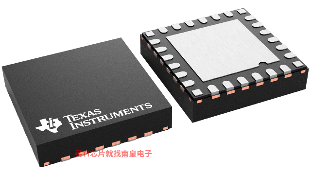
- Small footprint: 24-pin VQFN (4 mm × 4 mm)
- Function
- Clock generator
- Number of outputs
- 4
- Output frequency (Max) (MHz)
- 350
- Core supply voltage (V)
- 1.8, 2.5, 3.3
- Output supply voltage (V)
- 1.8, 2.5, 3.3
- Input type
- Universal input, LVCMOS, XTAL
- Output type
- LVCMOS, LVDS, HCSL
- Operating temperature range (C)
- -40 to 105
- Features
- I2C, Pin programmable, Integrated EEPROM, Serial interface
- Rating
- Catalog
CDCE6214的完整型号有:CDCE6214RGER、CDCE6214RGET,以下是这些产品的关键参数及官网采购报价:
CDCE6214RGER,工作温度:-40 to 105,封装:VQFN (RGE)-24,包装数量MPQ:3000个,MSL 等级/回流焊峰值温度:Level-2-260C-1 YEAR,引脚镀层/焊球材料:SN,TI官网CDCE6214RGER的批量USD价格:2.1(1000+)
CDCE6214RGET,工作温度:-40 to 105,封装:VQFN (RGE)-24,包装数量MPQ:250个,MSL 等级/回流焊峰值温度:Level-2-260C-1 YEAR,引脚镀层/焊球材料:SN,TI官网CDCE6214RGET的批量USD价格:2.52(1000+)

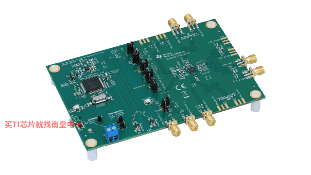
CDCE6214-Q1EVM CDCE6214-Q1EVM
The CDCE6214-Q1 evalution module (EVM) is an evaluation platform for the CDCE6214-Q1 ultra-low power clock generator. Thisevaluation module provides an USB-based interface to access the I2C bus to communicate with theCDCE6214-Q1. Pin control mode can set the device in a specific operation
PSPICE-FOR-TI 适用于 TI 设计和模拟工具的 PSpice
PSpice for TI 可提供帮助评估模拟电路功能的设计和仿真环境。此功能齐全的设计和仿真套件使用 Cadence 的模拟分析引擎。PSpice for TI 可免费使用,包括业内超大的模型库之一,涵盖我们的模拟和电源产品系列以及精选的模拟行为模型。借助PSpice for TI 的设计和仿真环境及其内置的模型库,您可对复杂的混合信号设计进行仿真。创建完整的终端设备设计和原型解决方案,然后再进行布局和制造,可缩短产品上市时间并降低开发成本。
在PSpice for TI 设计和仿真工具中,您可以搜索 TI (...)
CLOCK-TREE-ARCHITECT 时钟树架构编程软件
时钟树架构是一款时钟树综合工具,可根据您的系统要求生成时钟树解决方案,从而帮助您简化设计流程。该工具从庞大的时钟产品数据库中提取数据,然后生成系统级多芯片时钟解决方案。