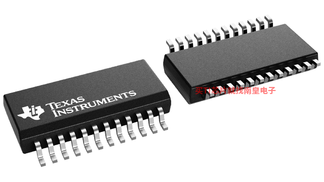
- 制造厂商:TI
- 产品类别:时钟和计时
- 技术类目:时钟发生器
- 功能描述:具有低至 10ps 以下可编程延迟线路的低抖动、基于 PLL 的倍频器和分频器
- 点击这里打开及下载CDCF5801A的技术文档资料
- TI代理渠道,提供当日发货、严格的质量标准,满足您的目标价格

The CDCF5801A provides clock multiplication from a reference clock (REFCLK) signal with the unique capability to delay or advance the CLKOUT/CLKOUTB with steps of only 1.3 mUI through a phase aligner. For every rising edge on the DLYCTRL pin the CLKOUT is delayed by a 1.3-mUI step size as long as the LEADLAG input detects a low signal at the time of the DLYCTRL rising edge. Similarly for every rising edge on the DLYCTRL pin the CLKOUT is advanced by a 1.3-mUI step size as long as the LEADLAG pin is high during the transition. This unique capability allows the device to phase align (zero delay) between CLKOUT/CLKOUTB and any one other CLK in the system by feeding the clocks that need to be aligned to the DLYCTRL and the LEADLAG pins. Also it provides the capability to program a fixed delay by providing the proper number of edges on the DLYCTRL pin, while strapping the LEADLAG pin to dc high or low. Further possible applications are:
- Aligning the rising edge of the output clock signal to the input clock rising edge
- Avoiding PLL instability in applications that require very long PLL feedback lines
- Isolation of jitter and digital switching noise
- Limitation of jitter in systems with good ppm frequency stability
The CDCF5801A has a fail-safe power up initialization state-machine which supports proper operation under all power up conditions.
The CDCF5801A provides clock multiplication and division from a reference clock (REFCLK) signal. The device is optimized to have extremely low jitter impact from input to output. The predivider pins MULT[0:1] and post-divider pins P[0:2] provide selection for frequency multiplication and division ratios, generating CLKOUT/CLOUTKB frequencies ranging from 25 MHz to 280 MHz with clock input references (REFCLK) ranging from 12.5 MHz to 240 MHz. See for detailed frequency support. The selection of pins MULT[0:1] and P[1:2] determines the multiplication value of 1, 2, 4, or 8. The CDCF5801A offers several power-down/ high-impedance modes, selectable by pins P0, STOPB and PWRDN. Another unique capability of the CDCF5801A is the high sensitivity and wide common-mode range of the clock-input pin REFCLK by varying the voltage on the VDDREF pin. The clock signal outputs CLKOUT and CLKOUTB can be used independently to generate single-ended clock signals. The CLKOUT/CLKOUTB outputs can also be combined to generate a differential output signal suitable for LVDS, LVPECL, or HSTL/SSTL signaling. The CDCF5801A is characterized for operation over free-air temperatures of -40°C to 85°C.
- Low-Jitter Clock Multiplier: ×1, ×2, ×4, ×8
- Fail-Safe Power Up Initialization
- Programmable Bidirectional Delay Steps of 1.3 mUI
- Output Frequency Range of 25 MHz to 280 MHz
- Input Frequency Range of 12.5 MHz to 240 MHz
- Low Jitter Generation
- Single-Ended REFCLK Input With Adjustable Trigger Level (Works With LVTTL, HSTL, and LVPECL)
- Differential/Single-Ended Output
- Output Can Drive LVPECL, LVDS, and LVTTL
- Three Power Operating Modes to Minimize Power
- Low Power Consumption (< 190 mW at 280 MHz/3.3 V)
- Packaged in a Shrink Small-Outline Package (DBQ)
- No External Components Required for PLL
- Spread Spectrum Clock Tracking Ability to Reduce EMI (SSC)
- APPLICATIONS
- Video Graphics
- Gaming Products
- Datacom
- Telecom
- Noise Cancellation Created by FPGAs
- Function
- Clock generator
- Number of outputs
- 1
- Output frequency (Max) (MHz)
- 280
- Core supply voltage (V)
- 3.3
- Output supply voltage (V)
- 3.3
- Input type
- HSTL, LVPECL, LVTTL
- Output type
- LVDS, LVPECL, LVTTL
- Operating temperature range (C)
- -40 to 85
- Features
- 3.3-V VCC/VDD, Pin programmable
- Rating
- Catalog
CDCF5801A的完整型号有:CDCF5801ADBQ、CDCF5801ADBQR,以下是这些产品的关键参数及官网采购报价:
CDCF5801ADBQ,工作温度:-40 to 85,封装:SSOP (DBQ)-24,包装数量MPQ:50个,MSL 等级/回流焊峰值温度:Level-2-260C-1 YEAR,引脚镀层/焊球材料:NIPDAU,TI官网CDCF5801ADBQ的批量USD价格:3.115(1000+)
CDCF5801ADBQR,工作温度:-40 to 85,封装:SSOP (DBQ)-24,包装数量MPQ:2500个,MSL 等级/回流焊峰值温度:Level-2-260C-1 YEAR,引脚镀层/焊球材料:NIPDAU,TI官网CDCF5801ADBQR的批量USD价格:2.596(1000+)

CDCF5801A IBIS Model
PSpice for TI 可提供帮助评估模拟电路功能的设计和仿真环境。此功能齐全的设计和仿真套件使用 Cadence 的模拟分析引擎。PSpice for TI 可免费使用,包括业内超大的模型库之一,涵盖我们的模拟和电源产品系列以及精选的模拟行为模型。借助?PSpice for TI 的设计和仿真环境及其内置的模型库,您可对复杂的混合信号设计进行仿真。创建完整的终端设备设计和原型解决方案,然后再进行布局和制造,可缩短产品上市时间并降低开发成本。
在?PSpice for TI 设计和仿真工具中,您可以搜索 TI (...)


