- 制造厂商:TI
- 产品类别:时钟和计时
- 技术类目:时钟缓冲器
- 功能描述:1:3 LVPECL 时钟缓冲器 + LVCMOS 输出 + 可编程分频器
- 点击这里打开及下载CDCM1804的技术文档资料
- TI代理渠道,提供当日发货、严格的质量标准,满足您的目标价格

The CDCM1804 clock driver distributes one pair of differential clock inputs to three pairs of LVPECL differential clock outputs Y[2:0] and Y[2:0], with minimum skew for clock distribution. The CDCM1804 is specifically designed for driving 50- transmission lines. Additionally, the CDCM1804 offers a single-ended LVCMOS output Y3. This output is delayed by 1.6 ns over the three LVPECL output stages to minimize noise impact during signal transitions.
The CDCM1804 has three control terminals, S0, S1, and S2, to select different output mode settings. The S[2:0] terminals are 3-level inputs and therefore allow up to 33 = 27 combinations. Additionally, an enable terminal (EN) is provided to disable or enable all outputs simultaneously. The EN terminal is a 3-level input as well and extends the number of settings to 2 × 27 = 54.
The CDCM1804 is characterized for operation from -40°C to 85°C.
For use in single-ended driver applications, the CDCM1804 also provides a VBB output terminal that can be directly connected to the unused input as a common-mode voltage reference.
- Distributes One Differential Clock Input to Three LVPECL Differential Clock Outputs and One LVCMOS Single-Ended Output
- Programmable Output Divider for Two LVPECL Outputs and LVCMOS Output
- Low-Output Skew 15 ps (Typical) for Clock-Distribution Applications for LVPECL Outputs; 1.6-ns Output Skew Between LVCMOS and LVPECL Transitions Minimizing Noise
- VCC Range 3 V-3.6 V
- Signaling Rate Up to 800-MHz LVPECL and 200-MHz LVCMOS
- Differential Input Stage for Wide Common-Mode Range
- Provides VBB Bias Voltage Output for Single-Ended Input Signals
- Receiver Input Threshold ±75 mV
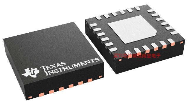
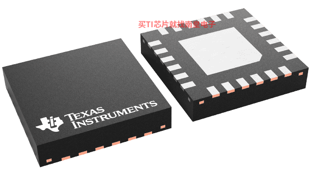
- 24-Terminal QFN Package (4 mm × 4 mm)
- Accepts Any Differential Signaling: LVDS, HSTL, CML, VML, SSTL-2, and Single-Ended: LVTTL/LVCMOS
- Function
- Clock divider, Fanout
- Additive RMS jitter (Typ) (fs)
- 150
- Output frequency (Max) (MHz)
- 800
- Number of outputs
- 3
- Output supply voltage (V)
- 3.3
- Core supply voltage (V)
- 3.3
- Output skew (ps)
- 30
- Features
- Pin programmable
- Operating temperature range (C)
- -40 to 85
- Rating
- Catalog
- Output type
- 1-LVCMOS No of outputs = 3 LVPECL, LVCMOS, LVPECL
- Input type
- LVPECL
CDCM1804的完整型号有:CDCM1804RGER、CDCM1804RGET,以下是这些产品的关键参数及官网采购报价:
CDCM1804RGER,工作温度:-40 to 85,封装:VQFN (RGE)-24,包装数量MPQ:3000个,MSL 等级/回流焊峰值温度:Level-2-260C-1 YEAR,引脚镀层/焊球材料:NIPDAU,TI官网CDCM1804RGER的批量USD价格:5.452(1000+)
CDCM1804RGET,工作温度:-40 to 85,封装:VQFN (RGE)-24,包装数量MPQ:250个,MSL 等级/回流焊峰值温度:Level-2-260C-1 YEAR,引脚镀层/焊球材料:NIPDAU,TI官网CDCM1804RGET的批量USD价格:6.542(1000+)

CDCM1804 IBIS Model
PSpice for TI 可提供帮助评估模拟电路功能的设计和仿真环境。此功能齐全的设计和仿真套件使用 Cadence 的模拟分析引擎。PSpice for TI 可免费使用,包括业内超大的模型库之一,涵盖我们的模拟和电源产品系列以及精选的模拟行为模型。借助?PSpice for TI 的设计和仿真环境及其内置的模型库,您可对复杂的混合信号设计进行仿真。创建完整的终端设备设计和原型解决方案,然后再进行布局和制造,可缩短产品上市时间并降低开发成本。
在?PSpice for TI 设计和仿真工具中,您可以搜索 TI (...)