- ���쳧�̣�TI
- ��Ʒ���ʱ�Ӻͼ�ʱ
- ������Ŀ��ʱ�Ӷ����������ͬ����
- ����������3.3V �����ܿ����� V ��ʱ��ͬ�����Ͷ���������
- ������������CDCM7005-SP�ļ����ĵ�����
- TI�����������ṩ���շ������ϸ������������������Ŀ��۸�

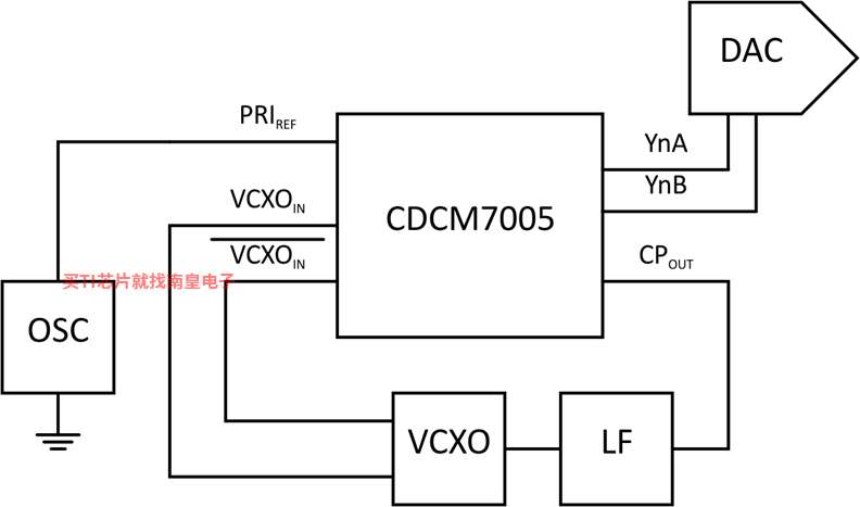
The CDCM7005-SP is a high-performance, low phase noise and low skew clock synchronizer that synchronizes a VCXO (voltage controlled crystal oscillator) or VCO (voltage controlled oscillator) frequency to one of the two reference clocks. The programmable pre-divider M and the feedback-dividers N and P give a high flexibility to the frequency ratio of the reference clock to VC(X)O as VC(X)O_IN / PRI_REF = (N × P) / M or VC(X)O_IN / SEC_REF = (N × P) / M.
VC(X)O_IN clock operates up to 2 GHz. Through the selection of external VC(X)O and loop filter components, the PLL loop bandwidth and damping factor can be adjust to meet different system requirements.
The CDCM7005-SP can lock to one of two reference clock inputs (PRI_REF and SEC_REF), supports frequency hold-over mode and fast-frequency-locking for fail-safe and increased system redundancy. The outputs of the CDCM7005-SP are user definable and can be any combination of up to five LVPECL outputs or up to 10 LVCMOS outputs. The LVCMOS outputs are arranged in pairs (Y0A:Y0B, Y1A:Y1B, Ω), so that each pair has the same frequency. But each output can be separately inverted and disabled. The built in synchronization latches ensure that all outputs are synchronized for low output skew.
All device settings, like outputs signaling, divider value, input selection, and many more, are programmable by SPI (3-wire serial peripheral interface). SPI allows individually control of the device settings.
The device operates in a 3.3-V environment and is characterized for operation from –55°C to 125°C (Tcase).
- High Performance LVPECL and LVCMOS PLL Clock Synchronizer
- Two Reference Clock Inputs (Primary and Secondary Clock) for Redundancy Support With Manual or Automatic Selection
- Accepts LVCMOS Input Frequencies Up to 200 MHz
- VCXO_IN Clock is Synchronized to One of the Two Reference Clocks
- VCXO_IN Frequencies Up to 2 GHz (LVPECL)
- Outputs can be a Combination of LVPECL and LVCMOS (Up to Five Differential LVPECL Outputs or Up to 10 LVCMOS Outputs)
- Output Frequency is Selectable by x1, /2, /3, /4, /6, /8, /16 on Each Output Individually
- Efficient Jitter Cleaning from Low PLL Loop Bandwidth
- Low Phase Noise PLL Core
- Programmable Phase Offset (PRI_REF and SEC_REF to Outputs)
- Wide Charge Pump Current Range From 200 ��A to 3 mA
- Analog and Digital PLL Lock Indication
- Provides VBB Bias Voltage Output for Single- Ended Input Signals (VCXO_IN)
- Frequency Hold Over Mode Improves Fail-Safe Operation
- Power-Up Control Forces LVPECL Outputs to Tri- State at VCC < 1.5 V
- SPI Controllable Device Setting
- 3.3-V Power Supply
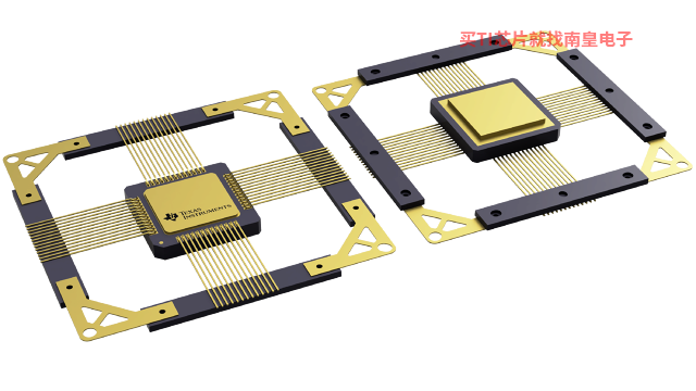
- High-Performance 52 Pin Ceramic Quad Flat Pack (HFG)
- Rad-Tolerant : 50 kRad (Si) TID
- QML-V Qualified, SMD 5962-07230
- Military Temperature Range: �C55��C to 125��C Tcase
- Engineering Evaluation (/EM) Samples are Available(1)
- Function
- Single-loop PLL
- Number of outputs
- 5
- Output frequency (Min) (MHz)
- 0
- Output frequency (Max) (MHz)
- 1500
- Input type
- LVCMOS (REF_CLK), LVPECL (VCXO_CLK)
- Output type
- LVCMOS, LVPECL
- Supply voltage (Min) (V)
- 3
- Supply voltage (Max) (V)
- 3.6
- Features
- Programmable Delay
- Operating temperature range (C)
- -55 to 125
CDCM7005-SP�������ͺ��У�5962-0723001VXC��CDCM7005HFG/EM����������Щ��Ʒ�Ĺؼ������������ɹ����ۣ�
5962-0723001VXC�������¶ȣ�-55 to 125����װ��CFP (HFG)-52����װ����MPQ��1����MSL �ȼ�/��������ֵ�¶ȣ�N/A for Pkg Type�����ŶƲ�/������ϣ�Call TI��TI����5962-0723001VXC������USD�۸�2750.066��1000+��
CDCM7005HFG/EM�������¶ȣ�0 to 0����װ��CFP (HFG)-52����װ����MPQ��1����MSL �ȼ�/��������ֵ�¶ȣ�N/A for Pkg Type�����ŶƲ�/������ϣ�Call TI��TI����CDCM7005HFG/EM������USD�۸�908��1000+��

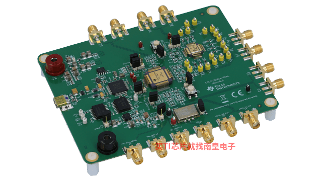
CDCM7005EVM-CVAL �� CDCM7005-SP ����ģ��
CDCM7005 ��һ������ܡ�����λ��������ƫ���ʱ��ͬ�������ɽ����ص�ѹ���ƾ������� (VC(X)O) Ƶ�����ⲿ�ο�ʱ�ӱ���ͬ����������������Ƶ�ʸߴ� 2 GHz��PLL ��·���������������ɽ��е��������㲻ͬ��ϵͳ��������ѡ���ⲿ VC(X)O����·�˲��������PFD ��Ƶ���Լ���ɱõ��������� LVPECL ����� LVCMOS ������е�ÿһ������ͨ����������ӿ� (SPI) ���б�̡��� SPI ���Ե�������Ƶ�ʺ�����/����ÿ�������״̬������ϵͳ��Ҫʹ���ⲿ��������磬��·�˲����� VC(X)O������˸� EVM (...)CDCM7005-SP EVM GUI
PSpice for TI ���ṩ��������ģ���·���ܵ���ƺͷ��滷�����˹�����ȫ����ƺͷ�����ʹ�� Cadence ��ģ��������档PSpice for TI �����ʹ�ã�����ҵ�ڳ����ģ�Ϳ�֮һ���������ǵ�ģ��͵�Դ��Ʒϵ���Լ���ѡ��ģ����Ϊģ�͡�����?PSpice for TI ����ƺͷ��滷���������õ�ģ�Ϳ⣬���ɶԸ��ӵĻ���ź���ƽ��з��档�����������ն��豸��ƺ�ԭ�ͽ��������Ȼ���ٽ��в��ֺ����죬�����̲�Ʒ����ʱ�䲢���Ϳ����ɱ���
��?PSpice for TI ��ƺͷ��湤���У����������� TI (...)
CLOCK-TREE-ARCHITECT �� ʱ�����ܹ��������
ʱ�����ܹ���һ��ʱ�����ۺϹ��ߣ��ɸ�������ϵͳҪ������ʱ��������������Ӷ���������������̡��ù��ߴ��Ӵ��ʱ�Ӳ�Ʒ���ݿ�����ȡ���ݣ�Ȼ������ϵͳ����оƬʱ�ӽ��������