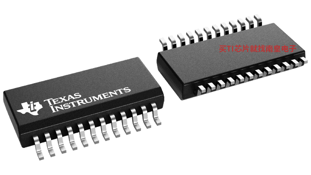
- 制造厂商:TI
- 产品类别:时钟和计时
- 技术类目:时钟缓冲器
- 功能描述:Direct Rambus 时钟发生器
- 点击这里打开及下载CDCR83A的技术文档资料
- TI代理渠道,提供当日发货、严格的质量标准,满足您的目标价格

The Direct Rambus clock generator (DRCG) provides the necessary clock signals to support a Direct Rambus memory subsystem. It includes signals to synchronize the Direct Rambus channel clock to an external system or processor clock. It is designed to support Direct Rambus memory on a desktop, workstation, server, and mobile PC motherboards. DRCG also provides an off-the-shelf solution for a broad range of Direct Rambus memory applications.
The DRCG provides clock multiplication and phase alignment for a Direct Rambus memory subsystem to enable synchronous communication between the Rambus channel and ASIC clock domains. In a Direct Rambus memory subsystem, a system clock source provides the REFCLK and PCLK clock references to the DRCG and memory controller, respectively. The DRCG multiplies REFCLK and drives a high-speed BUSCLK to RDRAMs and the memory controller. Gear ratio logic in the memory controller divides the PCLK and BUSCLK frequencies by ratios M and N such that PCLKM = SYNCLKN, where SYNCLK = BUSCLK/4. The DRCG detects the phase difference between PCLKM and SYNCLKN and adjusts the phase of BUSCLK such that the skew between PCLKM and SYNCLKN is minimized. This allows data to be transferred across the SYNCLK/PCLK boundary without incurring additional latency.
User control is provided by multiply and mode selection terminals. The multiply terminals provide selection of one of four clock frequency multiply ratios, generating BUSCLK frequencies ranging from 267 MHz to 400 MHz with clock references ranging from 33 MHz to 100 MHz. The mode select terminals can be used to select a bypass mode where the frequency multiplied reference clock is directly output to the Rambus channel for systems where synchronization between the Rambus clock and a system clock is not required. Test modes are provided to bypass the PLL and output REFCLK on the Rambus channel and to place the outputs in a high-impedance state for board testing.
The CDCR83A has a fail-safe power up initialization state-machine which supports proper operation under all power up conditions.
The CDCR83A is characterized for operation over free-air temperatures of –40°C to 85°C.
- 400-MHz Differential Clock Source for Direct Rambus? Memory Systems for an 800-MHz Data Transfer Rate
- Fail-Safe Power Up Initialization
- Synchronizes the Clock Domains of the Rambus Channel With an External System or Processor Clock
- Three Power Operating Modes to Minimize Power for Mobile and Other Power-Sensitive Applications
- Operates From a Single 3.3-V Supply and 120 mW at 300 MHz (Typ)
- Packaged in a Shrink Small-Outline Package (DBQ)
- Supports Frequency Multipliers: 4, 6, 8, 16/3
- No External Components Required for PLL
- Supports Independent Channel Clocking
- Spread Spectrum Clocking Tracking Capability to Reduce EMI
- Designed for Use With TI’s 133-MHz Clock Synthesizers CDC924 and CDC921
- Cycle-Cycle Jitter Is Less Than 50 ps at 400 MHz
- Certified by Gigatest Labs to Exceed the Rambus DRCG Validation Requirement
- Supports Industrial Temperature Range of –40°C to 85°C
DIRECT RAMBUS, Rambus are trademarks of Rambus Inc.
- Function
- Memory interface
- Additive RMS jitter (Typ) (fs)
- 50
- Output frequency (Max) (MHz)
- 400
- Number of outputs
- 1
- Output supply voltage (V)
- 3.3
- Core supply voltage (V)
- 3.3
- Output skew (ps)
- 0
- Features
- Rambus XDR
- Operating temperature range (C)
- -40 to 85
- Rating
- Catalog
- Output type
- CMOS
- Input type
- CMOS
CDCR83A的完整型号有:CDCR83ADBQR,以下是这些产品的关键参数及官网采购报价:
CDCR83ADBQR,工作温度:-40 to 85,封装:SSOP (DBQ)-24,包装数量MPQ:2500个,MSL 等级/回流焊峰值温度:Level-2-260C-1 YEAR,引脚镀层/焊球材料:NIPDAU,TI官网CDCR83ADBQR的批量USD价格:2.112(1000+)

CDCR83A IBIS Model
PSpice for TI 可提供帮助评估模拟电路功能的设计和仿真环境。此功能齐全的设计和仿真套件使用 Cadence 的模拟分析引擎。PSpice for TI 可免费使用,包括业内超大的模型库之一,涵盖我们的模拟和电源产品系列以及精选的模拟行为模型。借助?PSpice for TI 的设计和仿真环境及其内置的模型库,您可对复杂的混合信号设计进行仿真。创建完整的终端设备设计和原型解决方案,然后再进行布局和制造,可缩短产品上市时间并降低开发成本。
在?PSpice for TI 设计和仿真工具中,您可以搜索 TI (...)


