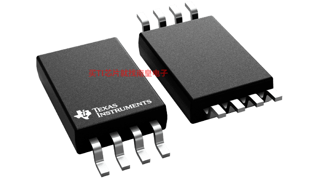
- 制造厂商:TI
- 产品类别:时钟和计时
- 技术类目:时钟发生器
- 功能描述:具有可选 SSC 的时钟缓冲器/时钟倍频器
- 点击这里打开及下载CDCS503的技术文档资料
- TI代理渠道,提供当日发货、严格的质量标准,满足您的目标价格

The CDCS503 is a spread spectrum capable, LVCMOS Input Clock Buffer with selectable frequency multiplication.
It shares major functionality with the CDCS502 but utilizes a LVCMOS input stage instead of the crystal input stage of the CDCS502. Also an Output Enable pin has been added to the CDCS503.
The device accepts a 3.3V LVCMOS signal at the input.
The input signal is processed by a PLL, whose output frequency is either equal to the input frequency or multiplied by the factor of 4.
The PLL is also able to spread the clock signal by ±0%, ±0.5%, ±1% or ±2% centered around the output clock frequency with a triangular modulation.
By this, the device can generate output frequencies between 8MHz and 108MHz with or without SSC.
A separate control pin can be used to enable or disable the output. The CDCS503 operates in 3.3V environment.
It is characterized for operation from –40°C to 85°C, and available in an 8-pin TSSOP package.
- Part of a Family of Easy to use Clock Generator Devices With Optional SSC
- Clock Multiplier With Selectable Output Frequency and Selectable SSC
- SSC Controllable via 2 External Pins
- ±0%, ±0.5%, ±1%, ±2% Center Spread
- Frequency Multiplication Selectable Between x1 or x4 With One External Control Pin
- Output Disable via Control Pin
- Single 3.3V Device Power Supply
- Wide Temperature Range –40°C to 85°C
- Low Space Consumption by 8 Pin TSSOP Package
- APPLICATIONS
- Consumer and Industrial Applications requiring EMI reduction through Spread Spectrum Clocking and/or Clock Multiplication
- Function
- Spread-spectrum clock generator
- Number of outputs
- 1
- Output frequency (Max) (MHz)
- 108
- Core supply voltage (V)
- 3.3
- Output supply voltage (V)
- 3.3
- Input type
- LVCMOS
- Output type
- LVCMOS
- Operating temperature range (C)
- -40 to 85
- Features
- Spread-spectrum clocking (SSC), Pin programmable
- Rating
- Catalog
CDCS503的完整型号有:CDCS503PW、CDCS503PWR,以下是这些产品的关键参数及官网采购报价:
CDCS503PW,工作温度:-40 to 85,封装:TSSOP (PW)-8,包装数量MPQ:150个,MSL 等级/回流焊峰值温度:Level-1-260C-UNLIM,引脚镀层/焊球材料:NIPDAU,TI官网CDCS503PW的批量USD价格:.546(1000+)
CDCS503PWR,工作温度:-40 to 85,封装:TSSOP (PW)-8,包装数量MPQ:2000个,MSL 等级/回流焊峰值温度:Level-1-260C-UNLIM,引脚镀层/焊球材料:NIPDAU,TI官网CDCS503PWR的批量USD价格:.455(1000+)

PSPICE-FOR-TI — 适用于 TI 设计和模拟工具的 PSpice
PSpice for TI 可提供帮助评估模拟电路功能的设计和仿真环境。此功能齐全的设计和仿真套件使用 Cadence 的模拟分析引擎。PSpice for TI 可免费使用,包括业内超大的模型库之一,涵盖我们的模拟和电源产品系列以及精选的模拟行为模型。借助?PSpice for TI 的设计和仿真环境及其内置的模型库,您可对复杂的混合信号设计进行仿真。创建完整的终端设备设计和原型解决方案,然后再进行布局和制造,可缩短产品上市时间并降低开发成本。
在?PSpice for TI 设计和仿真工具中,您可以搜索 TI (...)


