- 制造厂商:TI
- 产品类别:时钟和计时
- 技术类目:时钟缓冲器
- 功能描述:2.5V 锁相环路 DDR 时钟驱动器
- 点击这里打开及下载CDCVF857的技术文档资料
- TI代理渠道,提供当日发货、严格的质量标准,满足您的目标价格

The CDCVF857 is a high-performance, low-skew, low-jitter, zero-delay buffer that distributes a differential clock input pair (CLK, CLK) to 10 differential pairs of clock outputs (Y[0:9], Y[0:9]) and one differential pair of feedback clock outputs (FBOUT, FBOUT). The clock outputs are controlled by the clock inputs (CLK, CLK), the feedback clocks (FBIN, FBIN), and the analog power input (AVDD). When PWRDWN is high, the outputs switch in phase and frequency with CLK. When PWRDWN is low, all outputs are disabled to a high-impedance state (3-state) and the PLL is shut down (low-power mode). The device also enters this low-power mode when the input frequency falls below a suggested detection frequency that is below 20 MHz (typical 10 MHz). An input frequency detection circuit detects the low frequency condition and, after applying a >20-MHz input signal, this detection circuit turns the PLL on and enables the outputs.
When AVDD is strapped low, the PLL is turned off and bypassed for test purposes. The CDCVF857 is also able to track spread spectrum clocking for reduced EMI.
Because the CDCVF857 is based on PLL circuitry, it requires a stabilization time to achieve phase-lock of the PLL. This stabilization time is required following power up. The CDCVF857 is characterized for both commercial and industrial temperature ranges.
- Spread-Spectrum Clock Compatible
- Operating Frequency: 60 MHz to 220 MHz
- Low Jitter (Cycle-Cycle): ±35 ps
- Low Static Phase Offset: ±50 ps
- Low Jitter (Period): ±30 ps
- 1-to-10 Differential Clock Distribution (SSTL2)
- Best in Class for VOX = VDD/2 ±0.1 V
- Operates From Dual 2.6-V or 2.5-V Supplies
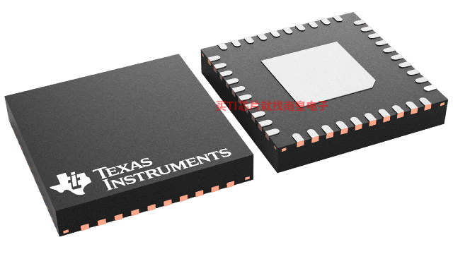
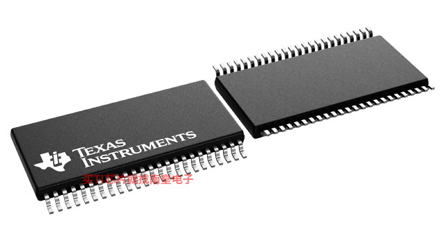
- Available in a 40-Pin MLF Package, 48-Pin TSSOP Package, 56-Ball MicroStar Junior? BGA Package
- Consumes < 100-μA Quiescent Current
- External Feedback Pins (FBIN, FBIN) Are Used to Synchronize the Outputs to the Input Clocks
- Meets/Exceeds JEDEC Standard (JESD82-1) For DDRI-200/266/333 Specification
- Meets/Exceeds Proposed DDRI-400 Specification (JESD82-1A)
- Enters Low-Power Mode When No CLK Input Signal Is Applied or PWRDWN Is Low
- APPLICATIONS
- DDR Memory Modules (DDR400/333/266/200)
- Zero-Delay Fan-Out Buffer
MicroStar Junior is a trademark of Texas Instruments.
- Function
- Zero-delay
- Additive RMS jitter (Typ) (fs)
- 30
- Output frequency (Max) (MHz)
- 220
- Number of outputs
- 10
- Output supply voltage (V)
- 1.7
- Core supply voltage (V)
- 2.5
- Output skew (ps)
- 75
- Features
- Spread spectrum clocking (SSC)
- Operating temperature range (C)
- -40 to 85
- Rating
- Catalog
- Output type
- LVTTL
- Input type
- LVTTL
CDCVF857的完整型号有:CDCVF857DGG、CDCVF857DGGR、CDCVF857RHAT、HPA00126DGGR,以下是这些产品的关键参数及官网采购报价:
CDCVF857DGG,工作温度:-40 to 85,封装:TSSOP (DGG)-48,包装数量MPQ:40个,MSL 等级/回流焊峰值温度:Level-2-260C-1 YEAR,引脚镀层/焊球材料:NIPDAU,TI官网CDCVF857DGG的批量USD价格:4.333(1000+)
CDCVF857DGGR,工作温度:-40 to 85,封装:TSSOP (DGG)-48,包装数量MPQ:2000个,MSL 等级/回流焊峰值温度:Level-2-260C-1 YEAR,引脚镀层/焊球材料:NIPDAU,TI官网CDCVF857DGGR的批量USD价格:3.666(1000+)
CDCVF857RHAT,工作温度:-40 to 85,封装:VQFN (RHA)-40,包装数量MPQ:250个,MSL 等级/回流焊峰值温度:Level-3-260C-168 HR,引脚镀层/焊球材料:NIPDAU,TI官网CDCVF857RHAT的批量USD价格:4.5(1000+)
HPA00126DGGR,工作温度:-40 to 85,封装:TSSOP (DGG)-48,包装数量MPQ:2000个,MSL 等级/回流焊峰值温度:-,引脚镀层/焊球材料:-,TI官网HPA00126DGGR的批量USD价格:3.666(1000+)

CDCVF857 IBIS Model
PSpice for TI 可提供帮助评估模拟电路功能的设计和仿真环境。此功能齐全的设计和仿真套件使用 Cadence 的模拟分析引擎。PSpice for TI 可免费使用,包括业内超大的模型库之一,涵盖我们的模拟和电源产品系列以及精选的模拟行为模型。借助?PSpice for TI 的设计和仿真环境及其内置的模型库,您可对复杂的混合信号设计进行仿真。创建完整的终端设备设计和原型解决方案,然后再进行布局和制造,可缩短产品上市时间并降低开发成本。
在?PSpice for TI 设计和仿真工具中,您可以搜索 TI (...)