- 制造厂商:TI
- 产品类别:数据转换器
- 技术类目:数模转换器 (DAC) - 高速数模转换器 (>10MSPS)
- 功能描述:双通道、14 位、275MSPS 数模转换器 (DAC)
- 点击这里打开及下载DAC5672的技术文档资料
- TI代理渠道,提供当日发货、严格的质量标准,满足您的目标价格

The DAC5672 device is a monolithic, dual-channel, 14-bit, high-speed DAC with on-chip voltage reference.
Operating with update rates of up to 275 MSPS, the DAC5672 offers exceptional dynamic performance, tight-gain, and offset matching characteristics that make the device well-suited in I/Q baseband or direct IF communication applications.
Each DAC has a high-impedance, differential-current output suitable for single-ended or differential analog-output configurations. External resistors allow scaling the full-scale output current for each DAC separately or together, typically between 2 mA and 20 mA. An accurate on-chip voltage reference is temperature-compensated and delivers a stable 1.2-V reference voltage. Optionally, an external reference may be used.
The DAC5672 has two, 14-bit, parallel input ports with separate clocks and data latches. For flexibility, the DAC5672 supports multiplexed data for each DAC on one port when operating in interleaved mode.
The DAC5672 is specifically designed for a differential transformer-coupled output with a 50-Ω doubly-terminated load. For a 20-mA full-scale output current, a 4:1 impedance ratio (resulting in an output power of 4 dBm) and 1:1 impedance ratio transformer (–2 dBm output power) are supported.
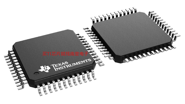
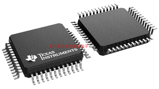
The DAC5672 is available in a 48-pin TQFP package. Pin compatibility between family members provides 12-bit (DAC5662) and 14-bit (DAC5672) resolutions. Furthermore, the DAC5672 is pin compatible to the DAC2904 and AD9767 dual DACs. The device is characterized for operation over the industrial temperature range from –40°C to 85°C.
- 14-Bit Dual Transmit Digital-to-Analog Converter (DAC)
- 275 MSPS Update Rate
- Single-Supply: 3 V to 3.6 V
- High Spurious-Free Dynamic Range (SFDR): 84 dBc at 5 MHz
- High Third-Order Two-Tone Intermodulation (IMD3): 79 dBc at 15.1 MHz and 16.1 MHz
- WCDMA Adjacent Channel Leakage Ratio (ACLR): 78 dB at Baseband
- WCDMA ACLR: 73 dB at 30.72 MHz
- Independent or Single Resistor Gain Control
- Dual or Interleaved Data
- On-Chip 1.2-V Reference
- Low Power: 330 mW
- Power-Down Mode: 9 mW
- Package: 48-Pin Thin-Quad Flat Pack (TQFP)
- Resolution (Bits)
- 14
- Number of DAC channels (#)
- 2
- Interface type
- Parallel CMOS
- Sample/update rate (MSPS)
- 275
- Features
- Low Power
- Rating
- Catalog
- Interpolation
- 1x
- Power consumption (Typ) (mW)
- 330
- SFDR (dB)
- 84
- Architecture
- Current Source
- Operating temperature range (C)
- -40 to 85
- Reference type
- Int
DAC5672的完整型号有:DAC5672IPFB、DAC5672IPFBR,以下是这些产品的关键参数及官网采购报价:
DAC5672IPFB,工作温度:-40 to 85,封装:TQFP (PFB)-48,包装数量MPQ:250个,MSL 等级/回流焊峰值温度:Level-2-260C-1 YEAR,引脚镀层/焊球材料:NIPDAU,TI官网DAC5672IPFB的批量USD价格:14.971(1000+)
DAC5672IPFBR,工作温度:-40 to 85,封装:TQFP (PFB)-48,包装数量MPQ:1000个,MSL 等级/回流焊峰值温度:Level-2-260C-1 YEAR,引脚镀层/焊球材料:NIPDAU,TI官网DAC5672IPFBR的批量USD价格:12.971(1000+)

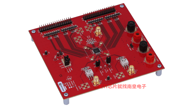
DAC5672EVM ― DAC5672 评估模块
This tool is designed to enable DAC5672 evaluation under various signals, reference and supply conditions.
DAC5672 IBIS Model (Rev. A)
PSpice for TI 可提供帮助评估模拟电路功能的设计和仿真环境。此功能齐全的设计和仿真套件使用 Cadence 的模拟分析引擎。PSpice for TI 可免费使用,包括业内超大的模型库之一,涵盖我们的模拟和电源产品系列以及精选的模拟行为模型。借助?PSpice for TI 的设计和仿真环境及其内置的模型库,您可对复杂的混合信号设计进行仿真。创建完整的终端设备设计和原型解决方案,然后再进行布局和制造,可缩短产品上市时间并降低开发成本。
在?PSpice for TI 设计和仿真工具中,您可以搜索 TI (...)
MATCHGAIN-CALC ― Wideband Comp Current Output DAC to SE Interface: Impr Matching for Gain & Compliance Volt Swing
NOTE: Calculator software is available when downloading the application note.- Click on "abstract" to view abstract of document.
- Open the ZIP file to extract the calculator tool.
- Open the PDF file to view the application note.
High-speed digital-to-analog converters (DACs) most often use a (...)
TIDA-00078 ― 具有 I/Q 校正的直接降压转换系统
TSW6011EVM 的现场可编程门阵列 (FPGA) 中实施的 I/Q 校正块可帮助用户在无线系统中采用直接降压转换接收器架构。I/Q 校正块包含一个单头盲算法,该算法可以校正零中频接收器系统中与频率无关的 I/Q 不平衡。除了 I/Q 校正块,FPGA 还包括一个数字增益块、一个数字功率测量块、两个内插块、一个 I/Q 偏移校正块和一个正交混频块。