- 制造厂商:TI
- 产品类别:数据转换器
- 技术类目:数模转换器 (DAC) - 高速数模转换器 (>10MSPS)
- 功能描述:14 位、400MSPS、2x-4x 内插数模转换器 (DAC)
- 点击这里打开及下载DAC5674的技术文档资料
- TI代理渠道,提供当日发货、严格的质量标准,满足您的目标价格

The DAC5674 is a 14-bit resolution high-speed digital-to-analog converter (DAC) with integrated 4x-interpolation filter, on-board clock multiplier, and on-chip voltage reference. The device has been designed for high-speed digital data transmission in wired and wireless communication systems, high-frequency direct-digital synthesis (DDS) and waveform reconstruction in test and measurement applications.
The 4x-interpolation filter is implemented as a cascade of two 2x-interpolation filters, each of which can be configured for either low-pass or high-pass response. This enables the user to select one of the higher order images present at multiples of the input data rate clock while maintaining a low date input rate. The resulting high IF output frequency allows the user to omit the conventional first mixer in heterodyne transmitter architectures and directly up-convert to RF using only one mixer, thereby reducing system complexity and costs.
In 4x-interpolation low-pass response mode, the DACs excellent spurious free dynamic range (SFDR) at intermediate frequencies located in the first Nyquist zone (up to 40 MHz) allows for multicarrier transmission in cellular base transceiver stations (BTS). The low-pass interpolation mode thereby relaxes image filter requirements by filtering out the images in the adjacent Nyquist zones.
The DAC5674 PLL clock multiplier controls all internal clocks for the digital filters and DAC core. The differential clock input and internal clock circuitry provides for optimum jitter performance. Sine wave clock input signal is supported. The PLL can be bypassed by an external clock running at the DAC core update rate. The clock divider of the PLL ensures that the digital filters operate at the correct clock frequencies.
The DAC5674 operates from an analog supply voltage of 3.3 V and a digital supply voltage of 1.8 V. The digital I/Os are 1.8-V and 3.3-V CMOS compatible. Power dissipation is 500 mW at maximum operating conditions. The DAC5674 provides a nominal full-scale differential current-output of 20 mA, supporting both single-ended and differential applications. The output current can be directly fed to the load with no additional external output buffer required. The device has been specifically designed for a differential transformer coupled output with a 50- doubly terminated load. For a 20-mA full-scale output current both a 4:1 impedance ratio (resulting in an output power of 4 dBm) and 1:1 impedance ratio transformer (–2-dBm output power) are supported. The latter configuration is preferred for optimum performance at high output frequencies and update rates.
An accurate on-chip 1.2-V temperature compensated bandgap reference and control amplifier allows the user to adjust the full-scale output current from 20 mA down to 2 mA. This provides 20-dB gain range control capabilities. Alternatively, an external reference voltage may be applied for maximum flexibility. The device features a SLEEP mode, which reduces the standby power to approximately 10 mW, thereby optimizing the power consumption for the system’s need.
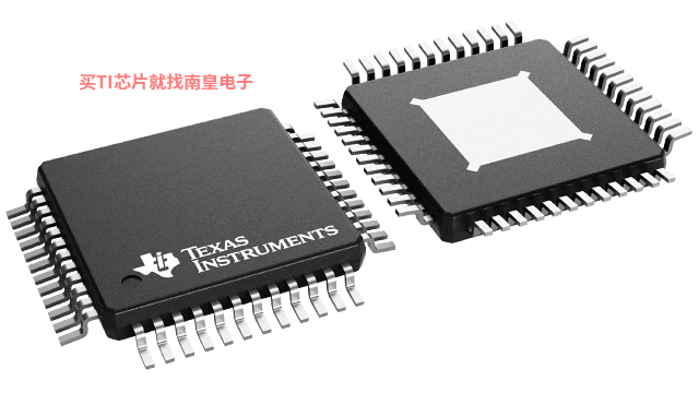
The DAC5674 is available in a 48-pin HTQFP Powerpad™ plastic quad flatpack package. The device is characterized for operation over the industrial temperature range of –40°C to 85°C.
- 200-MSPS Maximum Input Data Rate
- 400-MSPS Maximum Update Rate DAC
- 76-dBc SFDR Over Full First Nyquist Zone With Single Tone Input Signal (Fout = 21 MHz)
- 74-dBc ACPR W-CDMA at 15.36 MHz IF
- 69-dBc ACPR W-CDMA at 30.72 MHz IF
- Selectable 2x or 4x Interpolation Filter
- Linear Phase
- 0.05-dB Passband Ripple
- 80-dB Stopband Attenuation
- Stopband Transition 0.4-0.6 Fdata
- Interpolation Filters Configurable in Either Low-Pass or High-Pass Mode, Allows For Selection Higher Order Image
- On-chip 2x/4x PLL Clock Multiplier, PLL Bypass Mode
- Differential Scalable Current Outputs: 2 mA to 20 mA
- On-Chip 1.2-V Reference
- 1.8-V Digital and 3.3-V Analog Supply Operation
- 1.8/3.3-V CMOS Compatible Interface
- Power Dissipation: 435 mW at 400 MSPS
- Package: 48-Pin TQFP
- APPLICATIONS
- Cellular Base Transceiver Station Transmit Channel
- CDMA: W-CDMA, CDMA2000, IS-95
- TDMA: GSM, IS-136, EDGE/UWC-136
- Test and Measurement: Arbitrary Waveform Generation
- Direct Digital Synthesis (DDS)
- Cable Modem Termination System
- Cellular Base Transceiver Station Transmit Channel
Excel is a trademark of Microsoft Corporation. CommsDAC and PowerPAD are trademarks of Texas Instruments. All other trademarks are the property of their respective owners.
- Resolution (Bits)
- 14
- Number of DAC channels (#)
- 1
- Interface type
- Parallel CMOS
- Sample/update rate (MSPS)
- 400
- Features
- High Performance
- Rating
- Catalog
- Interpolation
- 2x, 4x
- Power consumption (Typ) (mW)
- 435
- SFDR (dB)
- 85
- Architecture
- Current Source
- Operating temperature range (C)
- -40 to 85
- Reference type
- Int
DAC5674的完整型号有:DAC5674IPHP、DAC5674IPHPR,以下是这些产品的关键参数及官网采购报价:
DAC5674IPHP,工作温度:-40 to 85,封装:HTQFP (PHP)-48,包装数量MPQ:250个,MSL 等级/回流焊峰值温度:Level-3-260C-168 HR,引脚镀层/焊球材料:NIPDAU,TI官网DAC5674IPHP的批量USD价格:24.011(1000+)
DAC5674IPHPR,工作温度:-40 to 85,封装:HTQFP (PHP)-48,包装数量MPQ:1000个,MSL 等级/回流焊峰值温度:Level-3-260C-168 HR,引脚镀层/焊球材料:NIPDAU,TI官网DAC5674IPHPR的批量USD价格:22.011(1000+)

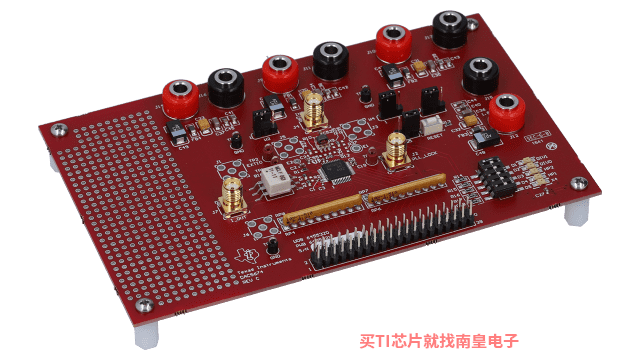
DAC5674EVM ― DAC5674 评估模块
DAC5674 is an evaluation module for DAC5674, a 400 MSPS digital to analog converter with 2x/4x interpolation. This evaluation module is designed to enable you to evaluate the device under various modes of operation.
DAC5674 IBIS Model
PSpice for TI 可提供帮助评估模拟电路功能的设计和仿真环境。此功能齐全的设计和仿真套件使用 Cadence 的模拟分析引擎。PSpice for TI 可免费使用,包括业内超大的模型库之一,涵盖我们的模拟和电源产品系列以及精选的模拟行为模型。借助?PSpice for TI 的设计和仿真环境及其内置的模型库,您可对复杂的混合信号设计进行仿真。创建完整的终端设备设计和原型解决方案,然后再进行布局和制造,可缩短产品上市时间并降低开发成本。
在?PSpice for TI 设计和仿真工具中,您可以搜索 TI (...)
MATCHGAIN-CALC ― Wideband Comp Current Output DAC to SE Interface: Impr Matching for Gain & Compliance Volt Swing
NOTE: Calculator software is available when downloading the application note.- Click on "abstract" to view abstract of document.
- Open the ZIP file to extract the calculator tool.
- Open the PDF file to view the application note.
High-speed digital-to-analog converters (DACs) most often use a (...)