- ���쳧�̣�TI
- ��Ʒ�������ת����
- ������Ŀ����ģת���� (DAC) - ������ģת���� (>10MSPS)
- ����������QMLV��150krad���մɡ�14 λ����ͨ����400MSPS DAC
- ������������DAC5675A-SP�ļ����ĵ�����
- TI�����������ṩ���շ������ϸ������������������Ŀ��۸�

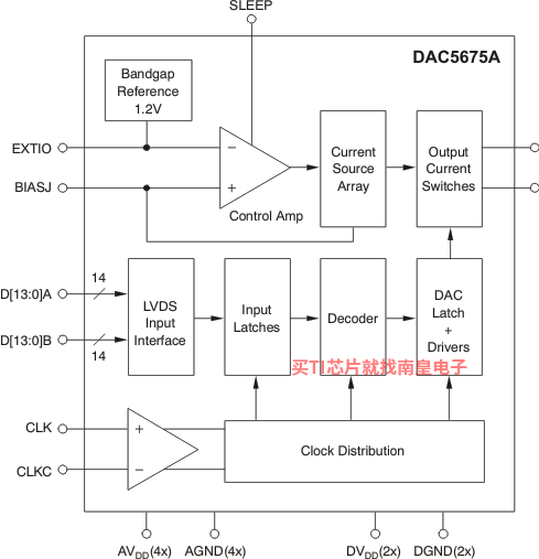
The DAC5675A-SP is a radiation-tolerant, 14-bit resolution high-speed digital-to-analog converter (DAC) primarily suited for space satellite applications. The DAC5675A-SP is designed for high-speed digital data transmission in wired and wireless communication systems, high-frequency direct digital synthesis (DDS), and waveform reconstruction in test and measurement applications. The DAC5675A-SP has excellent SFDR at high intermediate frequencies, which makes it well suited for multicarrier transmission in TDMA and CDMA based cellular base transceiver stations (BTSs).
The DAC5675A-SP operates from a single supply voltage of 3.3 V. Power dissipation is 660 mW at ƒCLK = 400 MSPS, ƒOUT = 70 MHz. The DAC5675A-SP provides a nominal full-scale differential current output of 20 mA, supporting both single-ended and differential applications. The output current can be directly fed to the load with no additional external output buffer required. The output is referred to the analog supply voltage AVDD.
The DAC5675A-SP includes a low-voltage differential signaling (LVDS) interface for high-speed digital data input. LVDS features a low differential voltage swing with a low constant power consumption across frequency, allowing for high-speed data transmission with low noise levels (low electromagnetic interference (EMI)).
LVDS is typically implemented in low-voltage digital CMOS processes, making it the ideal technology for high-speed interfacing between the DAC5675A-SP and high-speed low-voltage CMOS ASICs or FPGAs.
The DAC5675A-SP current-source-array architecture supports update rates of up to 400 MSPS. On-chip edge-triggered input latches provide for minimum setup and hold times, thereby relaxing interface timing.
The DAC5675A-SP is specifically designed for a differential transformer-coupled output with a 50-Ω doubly-terminated load. With the 20-mA full-scale output current, both a 4:1 impedance ratio (resulting in an output power of 4 dBm) and 1:1 impedance ratio transformer (–2 dBm) is supported. The last configuration is preferred for optimum performance at high output frequencies and update rates. The outputs are terminated to AVDD and have voltage compliance ranges from AVDD – 1 to AVDD + 0.3 V.
An accurate on-chip 1.2-V temperature-compensated bandgap reference and control amplifier allows the user to adjust this output current from 20 to 2 mA. This provides 20-dB gain range control capabilities. Alternatively, an external reference voltage may be applied. The DAC5675A-SP features a SLEEP mode, which reduces the standby power to approximately 18 mW.
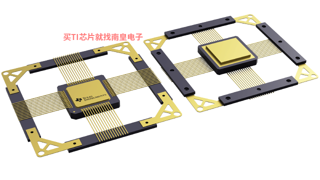
The DAC5675A-SP is available in a 52-pin ceramic nonconductive tie-bar package (HFG). The device is specified for operation over the military temperature range of –55°C to 125°C and W temperature range of –55°C to 115°C.
- QMLV (QML Class V) MIL-PRF-38535 Qualified, SMD 5962-07204
- 5962-0720401VXC �C Qualified over the Military Temperature Range (�C55��C to 125��C)
- 5962-0720402VXC �C Qualified over Reduced Temperature Range (�C55��C to 115��C) for Improved Dynamic Performance
- High-Performance 52-Pin Ceramic Quad Flat Pack (HFG)
- 400-MSPS Update Rate
- LVDS-Compatible Input Interface
- Spurious-Free Dynamic Range (SFDR) to Nyquist
- 69 dBc at 70 MHz IF, 400 MSPS
- W-CDMA Adjacent Channel Power Ratio (ACPR)
- 73 dBc at 30.72 MHz IF, 122.88 MSPS
- 71 dBc at 61.44 MHz IF, 245.76 MSPS
- Differential Scalable Current Outputs: 2 to 20 mA
- On-Chip 1.2-V Reference
- Single 3.3-V Supply Operation
- Power Dissipation: 660 mW at ?CLK = 400 MSPS, ?OUT = 20 MHz
- APPLICATIONS
- Radiation Hardened Digital to Analog (DAC) Applications
- Space Satellite RF Data Transmission
- Cellular Base Transceiver Station Transmit Channel:
- CDMA: WCDMA, CDMA2000, IS-95
- TDMA: GSM, IS-136, EDGE/GPRS
- Supports Single-Carrier and Multicarrier Applications
- Engineering Evaluation (/EM) Samples are Available(1)
(1) These units are intended for engineering evaluation only. They are processed to a non-compliant flow (for example, no burn-in) and are tested to temperature rating of 25��C only. These units are not suitable for qualification, production, radiation testing or flight use. Parts are not warranted for performance on full MIL specified temperature range of �C55��C to 125��C or operating life. All other trademarks are the property of their respective owners
- Resolution (Bits)
- 14
- Number of DAC channels (#)
- 1
- Interface type
- Parallel LVDS
- Sample/update rate (MSPS)
- 400
- Features
- Low Power
- Rating
- Space
- Interpolation
- 1x
- Power consumption (Typ) (mW)
- 660
- SFDR (dB)
- 82
- Architecture
- Current Sink
- Operating temperature range (C)
- -55 to 125, 25 to 25, -55 to 115
- Reference type
- Int
DAC5675A-SP�������ͺ��У�5962-0720401VXC��5962-0720402VXC��DAC5675AHFG/EM����������Щ��Ʒ�Ĺؼ������������ɹ����ۣ�
5962-0720401VXC�������¶ȣ�-55 to 125����װ��CFP (HFG)-52����װ����MPQ��1����MSL �ȼ�/��������ֵ�¶ȣ�N/A for Pkg Type�����ŶƲ�/������ϣ�Call TI��TI����5962-0720401VXC������USD�۸�6708.24��1000+��
5962-0720402VXC�������¶ȣ�-55 to 115����װ��CFP (HFG)-52����װ����MPQ��1����MSL �ȼ�/��������ֵ�¶ȣ�N/A for Pkg Type�����ŶƲ�/������ϣ�Call TI��TI����5962-0720402VXC������USD�۸�6708.24��1000+��
DAC5675AHFG/EM�������¶ȣ�25 to 25����װ��CFP (HFG)-52����װ����MPQ��1����MSL �ȼ�/��������ֵ�¶ȣ�N/A for Pkg Type�����ŶƲ�/������ϣ�Call TI��TI����DAC5675AHFG/EM������USD�۸�2098.95��1000+��

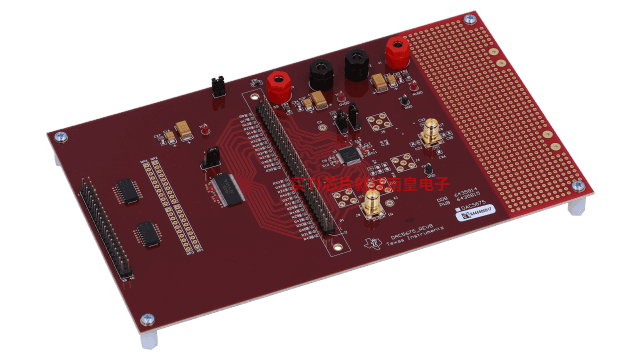
DAC5675AEVM �� DAC5675A ����ģ��
The DAC5675A EVM provides a platform for evaluating the DAC5675A, 14-bit 400MSPS digital to analog converters (DAC) family under various signal reference, and supply conditions.
DAC5675A-SP IBIS MODEL (Rev. A)
PSpice for TI ���ṩ��������ģ���·���ܵ���ƺͷ��滷�����˹�����ȫ����ƺͷ�����ʹ�� Cadence ��ģ��������档PSpice for TI �����ʹ�ã�����ҵ�ڳ����ģ�Ϳ�֮һ���������ǵ�ģ��͵�Դ��Ʒϵ���Լ���ѡ��ģ����Ϊģ�͡�����?PSpice for TI ����ƺͷ��滷���������õ�ģ�Ϳ⣬���ɶԸ��ӵĻ���ź���ƽ��з��档�����������ն��豸��ƺ�ԭ�ͽ��������Ȼ���ٽ��в��ֺ����죬�����̲�Ʒ����ʱ�䲢���Ϳ����ɱ���
��?PSpice for TI ��ƺͷ��湤���У����������� TI (...)