- 制造厂商:TI
- 产品类别:数据转换器
- 技术类目:数模转换器 (DAC) - 高速数模转换器 (>10MSPS)
- 功能描述:14 位 400MSPS 数模转换器 (DAC)
- 点击这里打开及下载DAC5675A的技术文档资料
- TI代理渠道,提供当日发货、严格的质量标准,满足您的目标价格

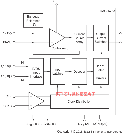
The DAC5675A is a 14-bit resolution high-speed digital-to-analog converter. The DAC5675A is designed for high-speed digital data transmission in wired and wireless communication systems, high-frequency direct-digital synthesis (DDS), and waveform reconstruction in test and measurement applications. The DAC5675A has excellent spurious-free dynamic range (SFDR) at high intermediate frequencies, which makes the DAC5675A well-suited for multicarrier transmission in TDMA- and CDMA-based cellular base transceiver stations (BTSs).
The DAC5675A operates from a single-supply voltage of 3.3 V. Power dissipation is 660 mW at fCLK = 400 MSPS, fOUT = 70 MHz. The DAC5675A provides a nominal full-scale differential current output of 20mA, supporting both single-ended and differential applications. The output current can be directly fed to the load with no additional external output buffer required. The output is referred to the analog supply voltage AVDD.
The DAC5675A comprises a low-voltage differential signaling (LVDS) interface for high-speed digital data input. LVDS features a low differential voltage swing with a low constant power consumption across frequency, allowing for high-speed data transmission with low noise levels; that is, with low electromagnetic interference (EMI). LVDS is typically implemented in low-voltage digital CMOS processes, making it the ideal technology for high-speed interfacing between the DAC5675A and high-speed low-voltage CMOS ASICs or FPGAs. The DAC5675A current-sink-array architecture supports update rates of up to 400MSPS. On-chip edge-triggered input latches provide for minimum setup and hold times, thereby relaxing interface timing.
The DAC5675A has been specifically designed for a differential transformer-coupled output with a 50 Ω doubly- terminated load. With the 20 mA full-scale output current, both a 4:1 impedance ratio (resulting in an output power of 4 dBm) and 1:1 impedance ratio transformer (–2 dBm) are supported. The last configuration is preferred for optimum performance at high output frequencies and update rates. The outputs are terminated to AVDD and have voltage compliance ranges from AVDD –1 to AVDD + 0.3 V.
An accurate on-chip 1.2-V temperature-compensated bandgap reference and control amplifier allows the user to adjust this output current from 20 mA down to 2 mA. This provides 20-dB gain range control capabilities. Alternatively, an external reference voltage may be applied. The DAC5675A features a SLEEP mode, which reduces the standby power to approximately 18 mW.
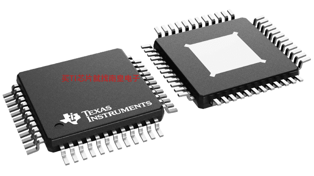
The DAC5675A is available in a 48-pin HTQFP thermally-enhanced PowerPad package. This package increases thermal efficiency in a standard size IC package. The device is characterized for operation over the industrial temperature range of –40°C to +85°C.
- 400MSPS Update Rate
- LVDS-Compatible Input Interface
- Spurious-Free Dynamic Range (SFDR) to Nyquist:
- 69dBc at 70MHz IF, 400MSPS
- W-CDMA Adjacent Channel Power Ratio (ACPR):
- 73dBc at 30.72MHz IF, 122.88MSPS
- 71dBc at 61.44MHz IF, 245.76MSPS
- Differential Scalable Current Sink Outputs: 2mA to 20mA
- On-Chip 1.2V Reference
- Single 3.3V Supply Operation
- Power Dissipation: 660mW at fCLK = 400MSPS, fOUT = 20MHz
- Package: 48-Pin HTQFP PowerPad, TJA = 28.8°C/W
- Resolution (Bits)
- 14
- Number of DAC channels (#)
- 1
- Interface type
- Parallel LVDS
- Sample/update rate (MSPS)
- 400
- Features
- High Performance
- Rating
- Catalog
- Interpolation
- 1x
- Power consumption (Typ) (mW)
- 660
- SFDR (dB)
- 88
- Architecture
- Current Sink
- Operating temperature range (C)
- -40 to 85
- Reference type
- Int
DAC5675A的完整型号有:DAC5675AIPHP,以下是这些产品的关键参数及官网采购报价:
DAC5675AIPHP,工作温度:-40 to 85,封装:HTQFP (PHP)-48,包装数量MPQ:250个,MSL 等级/回流焊峰值温度:Level-3-260C-168 HR,引脚镀层/焊球材料:NIPDAU,TI官网DAC5675AIPHP的批量USD价格:40.375(1000+)

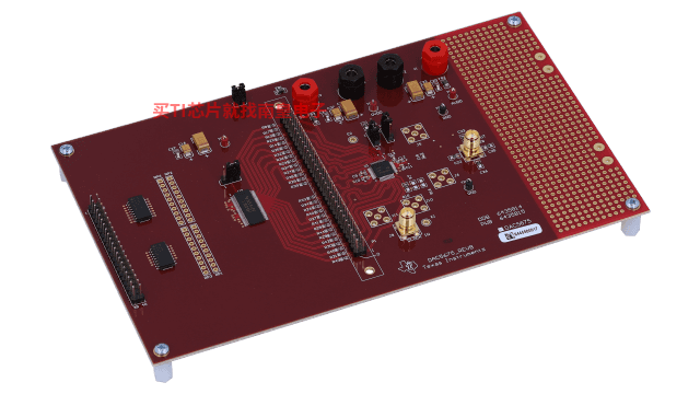
DAC5675AEVM ― DAC5675A 评估模块
The DAC5675A EVM provides a platform for evaluating the DAC5675A, 14-bit 400MSPS digital to analog converters (DAC) family under various signal reference, and supply conditions.
DAC5675A IBIS Model (Rev. A)
PSpice for TI 可提供帮助评估模拟电路功能的设计和仿真环境。此功能齐全的设计和仿真套件使用 Cadence 的模拟分析引擎。PSpice for TI 可免费使用,包括业内超大的模型库之一,涵盖我们的模拟和电源产品系列以及精选的模拟行为模型。借助?PSpice for TI 的设计和仿真环境及其内置的模型库,您可对复杂的混合信号设计进行仿真。创建完整的终端设备设计和原型解决方案,然后再进行布局和制造,可缩短产品上市时间并降低开发成本。
在?PSpice for TI 设计和仿真工具中,您可以搜索 TI (...)
MATCHGAIN-CALC ― Wideband Comp Current Output DAC to SE Interface: Impr Matching for Gain & Compliance Volt Swing
NOTE: Calculator software is available when downloading the application note.- Click on "abstract" to view abstract of document.
- Open the ZIP file to extract the calculator tool.
- Open the PDF file to view the application note.
High-speed digital-to-analog converters (DACs) most often use a (...)