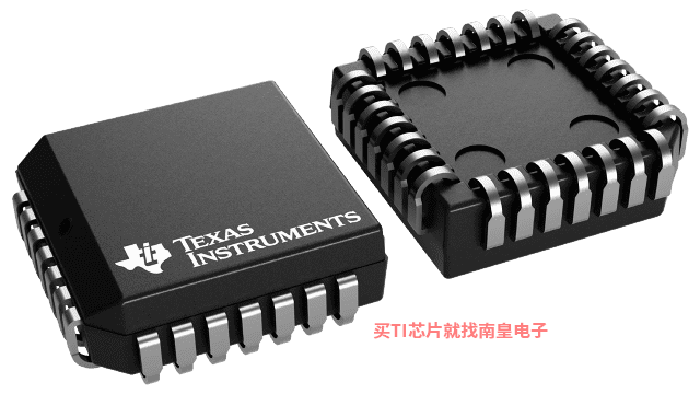
- 制造厂商:TI
- 产品类别:时钟和计时
- 技术类目:实时时钟 (RTC) 和计时器
- 功能描述:计时器控制外设 (TCP)
- 点击这里打开及下载DP8570A的技术文档资料
- TI代理渠道,提供当日发货、严格的质量标准,满足您的目标价格

The DP8570A is intended for use in microprocessor based systems where information is required for multi-tasking, data logging or general time of day/date information. This device is implemented in low voltage silicon gate microCMOS technology to provide low standby power in battery back-up environments. The circuit's architecture is such that it looks like a contiguous block of memory or I/O ports. The address space is organized as 2 software selectable pages of 32 bytes. This includes the Control Registers, the Clock Counters, the Alarm Compare RAM, the Timers and their data RAM, and the Time Save RAM. Any of the RAM locations that are not being used for their intended purpose may be used as general purpose CMOS RAM.
Time and date are maintained from 1/100 of a second to year and leap year in a BCD format, 12 or 24 hour modes. Day of week, day of month and day of year counters are provided. Time is controlled by an on-chip crystal oscillator requiring only the addition of the crystal and two capacitors. The choice of crystal frequency is program selectable.
Two independent multifunction 10 MHz 16-bit timers are provided. These timers operate in four modes. Each has its own prescaler and can select any of 8 possible clock inputs. Thus, by programming the input clocks and the timer counter values a very wide range of timing durations can be achieved. The range is from about 400 ns (4.915 MHz oscillator) to 65,535 seconds (18 hrs., 12 min.).
Power failure logic and control functions have been integrated on chip. This logic is used by the TCP to issue a power fail
interrupt, and lock out the µp interface. The time power fails may be logged into RAM automatically when VBB > VCC. Additionally, two supply pins are provided. When VBB > VCC, internal circuitry will automatically switch from the main supply to the battery supply. Status bits are provided to indicate initial application of battery power, system power, and low battery detect.
- Full function real time clock/calendar
- 12/24 hour mode timekeeping
- Day of week and day of years counters
- Four selectable oscillator frequencies
- Parallel Resonant Oscillator
- Two 16-bit timers
- 10 MHz external clock frequency
- Programmable multi-function output
- Flexible re-trigger facilities
- Power fail features
- Internal power supply switch to external battery
- Power Supply Bus glitch protection
- Automatic log of time into RAM at power failure
- On-chip interrupt structure
- Periodic, alarm, timer and power fail interrupts
- Up to 44 bytes of CMOS RAM
- INTR/MFO/T1 pins programmable High/Low and push-pull or open drain
TRI-STATE? is a registered trademark of National Semiconductor Corporation.
(size: 390486) WebDIRECT? SearchWebDIRECT? is a trademark of Coris, Inc., a wholly-owned subsidiary of R.R. Donnelley & Sons Company.
How to download and view our Data Sheets Our Data Sheets and other documents are available for downloading in the Portable Document Format (PDF). You can view and print these documents using the Adobe Acrobat Reader. If you do not already have Adobe Acrobat Reader installed and configured on your system, then click here.
Copyright ? 1995 National Semiconductor Corporation Learn About and Influence The Site
- Iq (Typ) (uA)
- 260
- Features
- 10-MHz external clock frequency, 12/24 hour, Parallel bus interface
- Rating
- Catalog
- Operating temperature range (C)
- -40 to 85
- Supply voltage (Max) (V)
- 5.5
- Supply voltage (Min) (V)
- 4.5
DP8570A的完整型号有:DP8570AV/NOPB、DP8570AVX/NOPB,以下是这些产品的关键参数及官网采购报价:
DP8570AV/NOPB,工作温度:-40 to 85,封装:PLCC (FN)-28,包装数量MPQ:35个,MSL 等级/回流焊峰值温度:Level-2A-245C-4 WEEK,引脚镀层/焊球材料:SN,TI官网DP8570AV/NOPB的批量USD价格:17.13(1000+)
DP8570AVX/NOPB,工作温度:-40 to 85,封装:PLCC (FN)-28,包装数量MPQ:750个,MSL 等级/回流焊峰值温度:Level-2A-245C-4 WEEK,引脚镀层/焊球材料:SN,TI官网DP8570AVX/NOPB的批量USD价格:15.13(1000+)

PSPICE-FOR-TI ― 适用于 TI 设计和模拟工具的 PSpice
PSpice for TI 可提供帮助评估模拟电路功能的设计和仿真环境。此功能齐全的设计和仿真套件使用 Cadence 的模拟分析引擎。PSpice for TI 可免费使用,包括业内超大的模型库之一,涵盖我们的模拟和电源产品系列以及精选的模拟行为模型。借助?PSpice for TI 的设计和仿真环境及其内置的模型库,您可对复杂的混合信号设计进行仿真。创建完整的终端设备设计和原型解决方案,然后再进行布局和制造,可缩短产品上市时间并降低开发成本。
在?PSpice for TI 设计和仿真工具中,您可以搜索 TI (...)


