- ���쳧�̣�TI
- ��Ʒ���ʱ�Ӻͼ�ʱ
- ������Ŀ��ʱ�Ӷ����������ͬ����
- ��������������˫���� PLL �ͼ���ʽ 2.5GHz VCO �ĵ�����ʱ�Ӷ���������
- ������������LMK04806�ļ����ĵ�����
- TI�����������ṩ���շ������ϸ������������������Ŀ��۸�

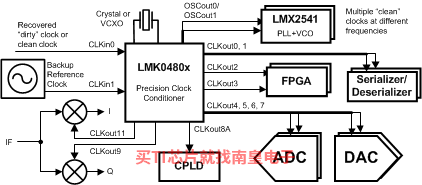
The LMK0480x family is the industry’s highest performance clock conditioner with superior clock jitter cleaning, generation, and distribution with advanced features to meet next generation system requirements. The dual loop PLLatinum architecture is capable of 111 fs rms jitter (12 kHz to 20 MHz) using a low noise VCXO module or sub-200 fs rms jitter (12 kHz to 20 MHz) using a low cost external crystal and varactor diode.
The dual loop architecture consists of two high-performance phase-locked loops (PLL), a low-noise crystal oscillator circuit, and a high-performance voltage controlled oscillator (VCO). The first PLL (PLL1) provides low-noise jitter cleaner functionality while the second PLL (PLL2) performs the clock generation. PLL1 can be configured to either work with an external VCXO module or the integrated crystal oscillator with an external tunable crystal and varactor diode. When paired with a very narrow loop bandwidth, PLL1 uses the superior close-in phase noise (offsets below 50 kHz) of the VCXO module or the tunable crystal to clean the input clock. The output of PLL1 is used as the clean input reference to PLL2 where it locks the integrated VCO. The loop bandwidth of PLL2 can be optimized to clean the far-out phase noise (offsets above 50 kHz) where the integrated VCO outperforms the VCXO module or tunable crystal used in PLL1.
- Ultra-Low RMS Jitter Performance
- 111 fs RMS Jitter (12 kHz to 20 MHz)
- 123 fs RMS Jitter (100 Hz to 20 MHz)
- Dual Loop PLLatinum? PLL Architecture
- PLL1
- Integrated Low-Noise Crystal Oscillator Circuit
- Holdover Mode when Input Clocks are Lost
- Automatic or Manual Triggering/Recovery
- PLL2
- Normalized PLL Noise Floor of �C227 dBc/Hz
- Phase Detector Rate up to 155 MHz
- OSCin Frequency-Doubler
- Integrated Low-Noise VCO
- 2 Redundant Input Clocks with LOS
- Automatic and Manual Switch-Over Modes
- 50 % Duty Cycle Output Divides, 1 to 1045 (Even and Odd)
- 12 LVPECL, LVDS, or LVCMOS Programmable Outputs
- Digital Delay: Fixed or Dynamically Adjustable
- 25 ps Step Analog Delay Control.
- 14 Differential Outputs. Up to 26 Single Ended.
- Up to 6 VCXO/Crystal Buffered Outputs
- Clock Rates of up to 1536 MHz
- 0-Delay Mode
- Three Default Clock Outputs at Power Up
- Multi-Mode: Dual PLL, Single PLL, and Clock Distribution
- Industrial Temperature Range: �C40 to 85��C
- 3.15-V to 3.45-V Operation
- 2 Dedicated Buffered/Divided OSCin Clocks
- Package: 64-Pin WQFN (9.0 �� 9.0 �� 0.8 mm)
- Function
- Cascaded PLLs
- Number of outputs
- 14
- RMS jitter (fs)
- 111
- Output frequency (Min) (MHz)
- 0.22
- Output frequency (Max) (MHz)
- 2600
- Input type
- LVCMOS, LVDS, LVPECL
- Output type
- LVCMOS, LVDS, LVPECL
- Supply voltage (Min) (V)
- 3.15
- Supply voltage (Max) (V)
- 3.45
- Features
- 0 Delay
- Operating temperature range (C)
- -40 to 85
LMK04806�������ͺ��У�LMK04806BISQ/NOPB��LMK04806BISQE/NOPB��LMK04806BISQX/NOPB����������Щ��Ʒ�Ĺؼ������������ɹ����ۣ�
LMK04806BISQ/NOPB�������¶ȣ�-40 to 85����װ��WQFN (NKD)-64����װ����MPQ��1000����MSL �ȼ�/��������ֵ�¶ȣ�Level-3-260C-168 HR�����ŶƲ�/������ϣ�SN��TI����LMK04806BISQ/NOPB������USD�۸�10.106��1000+��
LMK04806BISQE/NOPB�������¶ȣ�-40 to 85����װ��WQFN (NKD)-64����װ����MPQ��250����MSL �ȼ�/��������ֵ�¶ȣ�Level-3-260C-168 HR�����ŶƲ�/������ϣ�SN��TI����LMK04806BISQE/NOPB������USD�۸�10.106��1000+��
LMK04806BISQX/NOPB�������¶ȣ�-40 to 85����װ��WQFN (NKD)-64����װ����MPQ��2000����MSL �ȼ�/��������ֵ�¶ȣ�Level-3-260C-168 HR�����ŶƲ�/������ϣ�SN��TI����LMK04806BISQX/NOPB������USD�۸�8.422��1000+��

DAC34SH84EVM �� DAC34SH84 ����ģ��
The DAC34SH84EVM is a circuit board that allows designers to evaluate the performance of Texas Instruments' four-channel, ultra-low power, 16-bit, 1.5 GSPS DAC34SH84 digital-to-analog converter (DAC) with 32-bit wide DDR LVDS data input, integrated 2x/4x/8x/16x interpolation filters, 32-bit NCO and (...)
LMK04806BEVAL �� ����˫���� PLL �ͼ��� 2.5 GHz VCO ��ʱ�Ӷ���������
The LMK04800 family is the industry's highest performance clock conditioner with superior clock jitter cleaning, generation, and distribution with advanced features to meet next generation system requirements. The dual loop PLLatinum? architecture enables 111 fs rms jitter (12 kHz to 20 MHz) using (...)
TSW1265EVM �� ����˫·�������ο���ƺ�����ƽ̨
TSW1265EVM ��һ�����˫·�������ο���ƺ�����ƽ̨���ź���ͨ��˫ͨ���±�Ƶ��Ƶ����LMH6521 ˫ͨ�� DVGA���� ADS4249 14 λ 250 MSPS ADC ��������Ƶ��λ��ת����TSW1265EVM ������ LMK04800 ˫ PLL ʱ�Ӷ���������ͷ������������ṩ���ص�������ʱ������������ṩ���� GUI �������� ADS4249 �� LMK04800 �������á���ͨ�� GUI ��ͨ������ FPGA �ĸ������������� LMH6521 DVGA ���档EVM �ʺ��� TSW1400EVM Ѷ��ߢȡ�Ͳ�����·�����ʹ�ã���ߢȡ ADS4249 (...)
TSW3084EVM �� ������Ƶ�ź�������ģ��
TSW3084EVM ����ģ��Ϊ��·�壬������ϵͳ�����Ա���� LMK04806B ������ʱ�ӷ�����/������������������������ (TI) �����ź����������ܡ���Ϊ����ʹ�õ�������Ƶ������������TSW3084EVM ��������Ϊ DAC3484 ��ģת���� (DAC) �ṩ��ʱ�� LMK04806B���Լ������ɽ����� 4 ͨ�� DAC �� I/Q ����ϱ�ƵΪ��Ƶ�ز��� TRF3705��
DAC3484 ����ͨ�������� 16 λ 1.25 GSPS DAC��������Ч�Ķ�·���õ� 16 λ�����ߣ���ʵ��ÿ�� DAC ��������Ϊ 312MSPS��
TRF3705 �Ǹ����ܸ�����Ƶ�������������ΧΪ (...)
TSW30H84EVM �� ������Ƶ�ź�������ģ��
TSW30H84EVM ����ģ��Ϊ��·�壬������ϵͳ�����Ա���� LMK04806B����μ� LMK04800��������ʱ�ӷ�����/������������������������ (TI) �����ź���·�������ܡ���Ϊ����ʹ�õ�������Ƶ������������TSW30H84EVM ��������Ϊ DAC34H84 ��ģת���� (DAC) �ṩ��ʱ�� LMK04806B����μ� LMK04800�����Լ������ɽ����� 4 ͨ�� DAC �� I/Q ����ϱ�ƵΪ��Ƶ�ز��� TRF3705��
DAC34H84 ����ͨ�������� 16 λ 1.25 GSPS DAC���������ͼ������Ϊ 625MSPS/DAC��
TRF3705 (...)
TSW30SH84EVM �� ������Ƶ�ź�������ģ��
TSW30SH84EVM ����ģ��Ϊ��·�壬������ϵͳ�����Ա���� LMK04800 ������ʱ�ӷ�����/������������������������ (TI) �����ź����������ܡ���Ϊ����ʹ�õ�������Ƶ������������TSW30SH84EVM ��������Ϊ DAC34SH84 ��ģת���� (DAC) �ṩ��ʱ�� LMK04800���Լ������ɽ����� 4 ͨ�� DAC �� I/Q ����ϱ�ƵΪ��Ƶ�ز��� TRF3705��
DAC34SH84 ����ͨ�������� 16 λ 1.5 GSPS DAC���������ͼ������Ϊ 750MSPS/DAC��
TRF3705 �Ǹ����ܸ�����Ƶ�������������ΧΪ 300 MHz �� 4 (...)
CLOCKDESIGNTOOL �� ʱ����ƹ��� - ��·�˲������������� + ����
The Clock Design Tool software helps with part selection, loop filter design and simulation of timing device solutions. When you enter desired output frequencies and a reference frequency (optional), the tool provides TI devices to meet the specified requirements, divider values and a recommended (...)TSW308x EVM Software (Rev. B)
The CodeLoader 4 software is used to program the LMX PLLs and LMK timing devices through either the USB or line print terminal (LPT) port of a computer. This software also provides information on how to program the device by showing the bits that are actually sent.Which software do I use?
Product
(...)
LMK04806 IBIS Model (Rev. C)
PSpice for TI ���ṩ��������ģ���·���ܵ���ƺͷ��滷�����˹�����ȫ����ƺͷ�����ʹ�� Cadence ��ģ��������档PSpice for TI �����ʹ�ã�����ҵ�ڳ����ģ�Ϳ�֮һ���������ǵ�ģ��͵�Դ��Ʒϵ���Լ���ѡ��ģ����Ϊģ�͡�����?PSpice for TI ����ƺͷ��滷���������õ�ģ�Ϳ⣬���ɶԸ��ӵĻ���ź���ƽ��з��档�����������ն��豸��ƺ�ԭ�ͽ��������Ȼ���ٽ��в��ֺ����죬�����̲�Ʒ����ʱ�䲢���Ϳ����ɱ���
��?PSpice for TI ��ƺͷ��湤���У����������� TI (...)
CLOCK-TREE-ARCHITECT �� ʱ�����ܹ��������
ʱ�����ܹ���һ��ʱ�����ۺϹ��ߣ��ɸ�������ϵͳҪ������ʱ��������������Ӷ���������������̡��ù��ߴ��Ӵ��ʱ�Ӳ�Ʒ���ݿ�����ȡ���ݣ�Ȼ������ϵͳ����оƬʱ�ӽ��������TSW4806EVM Design Package Board rev A
�˲ο���������� TSW3100 �źŷ��������ʹ�� TSW3085EVM �Բ��� LTE �����źŵ������ŵ����ʱ� (ACPR) �����ʸ������ (EVM) ������ͨ��ʹ�� TSW3100 LTE GUI���ɽ��źż��ص��� DAC3482��TRF3705 �� LMK04806 ���ɵ� TSW3085EVM��TIDA-00072 �� ����������Ƶ���ͽ������
TSW308x ���ܹ����� 600 MHz ������ƵƵ�Ŀ�������/��Ƶת�����������������ʾ������ϵͳ�ṩ��ʾ�����ʹ�� DAC34x8x��TRF3705 IQ �������� LMK0480x ��ʵ��Ŀ�ꡣ�˲ο� EVM ����˿�����Ƶ�²�������խ���Ϳ����źŵ��źŷ��������� TSW1400EVM����������ṩ����β������ϱ��� WCDMA �����źŵ�����ʾ����