- ���쳧�̣�TI
- ��Ʒ���ʱ�Ӻͼ�ʱ
- ������Ŀ��ʱ�ӻ�����
- ����������8 ͨ����� LVDS 1.8V��2.5V �� 3.3V ������
- ������������LMK1D1208�ļ����ĵ�����
- TI�����������ṩ���շ������ϸ������������������Ŀ��۸�

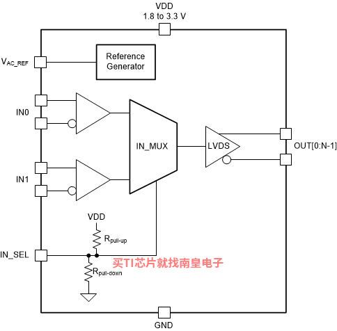
The LMK1D120x clock buffer distributes one of two selectable clock inputs (IN0 and IN1) to 4 or 8 pairs of differential LVDS clock outputs (OUT0 through OUT7) with minimum skew for clock distribution. The LMK1D12x family can accept two clock sources into an input multiplexer. The inputs can either be LVDS, LVPECL, LP-HCSL, HCSL, CML or LVCMOS.
The LMK1D12x is specifically designed for driving 50-Ω transmission lines. In case of driving the inputs in single-ended mode, the appropriate bias voltage as shown in Figure 8-6 must be applied to the unused negative input pin.
The IN_SEL pin selects the input which is routed to the outputs. If this pin is left open, it disables the outputs (logic low). The part supports a fail-safe function. The device further incorporates an input hysteresis which prevents random oscillation of the outputs in the absence of an input signal.
The device operates in 1.8-V or 2.5-V or 3.3-V supply environment and is characterized from –40°C to 105°C (ambient temperature). The LMK1D12x package variant is shown in the table below:
- High-performance LVDS clock buffer family with 2 inputs and 4 (2:4) or 8 (2:8) outputs.
- Output frequency up to 2 GHz.
- Supply voltage: 1.71 V to 3.465 V
- Low additive jitter: < maximum 60 fs RMS in 12-kHz to 20-MHz at 156.25 MHz
-
Very low phase noise floor: �C164 dBc/Hz (typical)
-
-
Very low propagation delay: < 575 ps maximum
-
Output skew: 20 ps maximum
- Universal inputs accept LVDS, LVPECL, LVCMOS, LP-HCSL, HCSL and CML inputs
- LVDS reference voltage, VAC_REF, available for capacitive-coupled inputs
- Industrial temperature range: �C40��C to 105��C
- Packages available:
-
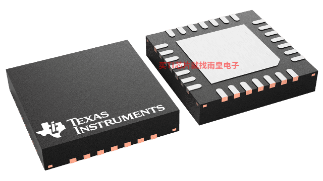
LMK1D1204: 3-mm �� 3-mm, 16-pin VQFN (RGT)
-
LMK1D1208: 5-mm �� 5-mm, 28-pin VQFN (RHD)
-
- Function
- Clock buffer, Differential
- Additive RMS jitter (Typ) (fs)
- 50
- Output frequency (Max) (MHz)
- 2000
- Number of outputs
- 8
- Output supply voltage (V)
- 1.8, 2.5, 3.3
- Core supply voltage (V)
- 1.8, 2.5, 3.3
- Output skew (ps)
- 20
- Features
- 2:8 fanout, Universal inputs
- Operating temperature range (C)
- -40 to 105
- Rating
- Catalog
- Output type
- LVDS
- Input type
- HCSL, LP-HCSL, LVCMOS, LVDS, LVPECL
LMK1D1208�������ͺ��У�LMK1D1208RHDR��LMK1D1208RHDT����������Щ��Ʒ�Ĺؼ������������ɹ����ۣ�
LMK1D1208RHDR�������¶ȣ�-40 to 105����װ��VQFN (RHD)-28����װ����MPQ��3000����MSL �ȼ�/��������ֵ�¶ȣ�Level-2-260C-1 YEAR�����ŶƲ�/������ϣ�NIPDAU��TI����LMK1D1208RHDR������USD�۸�4.279��1000+��
LMK1D1208RHDT�������¶ȣ�-40 to 105����װ��VQFN (RHD)-28����װ����MPQ��250����MSL �ȼ�/��������ֵ�¶ȣ�Level-2-260C-1 YEAR�����ŶƲ�/������ϣ�NIPDAU��TI����LMK1D1208RHDT������USD�۸�5.135��1000+��

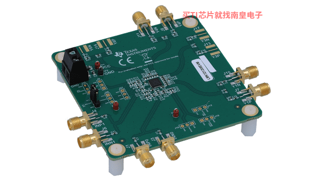
LMK1D1208EVM �� ������ LMK1D1208 �Ͷ��� 2:8 LVDS �ȳ�������������ģ��
LMK1D1208 ��һ������ܡ����Ӷ��� LVDS ʱ�ӻ����������������������Ͱ˸� LVDS �����������ģ�� (EVM) ּ����ʾ LMK1D1208 �ĵ������ܣ������������� LMK1Dxxxx ϵ���е����� 28 ����������Ϊ��ʵ�ֳ�ɫ���ܣ�LMK1D1208EVM �䱸�� 50�� SMA ���������迹���� 50�� �������ߡ�LMK1DX IBIS Model (Rev. A)
PSpice for TI ���ṩ��������ģ���·���ܵ���ƺͷ��滷�����˹�����ȫ����ƺͷ�����ʹ�� Cadence ��ģ��������档PSpice for TI �����ʹ�ã�����ҵ�ڳ����ģ�Ϳ�֮һ���������ǵ�ģ��͵�Դ��Ʒϵ���Լ���ѡ��ģ����Ϊģ�͡�����?PSpice for TI ����ƺͷ��滷���������õ�ģ�Ϳ⣬���ɶԸ��ӵĻ���ź���ƽ��з��档�����������ն��豸��ƺ�ԭ�ͽ��������Ȼ���ٽ��в��ֺ����죬�����̲�Ʒ����ʱ�䲢���Ϳ����ɱ���
��?PSpice for TI ��ƺͷ��湤���У����������� TI (...)