- 制造厂商:TI
- 产品类别:时钟和计时
- 技术类目:时钟缓冲器
- 功能描述:40MHz 双路时钟缓冲器
- 点击这里打开及下载LMV112的技术文档资料
- TI代理渠道,提供当日发货、严格的质量标准,满足您的目标价格

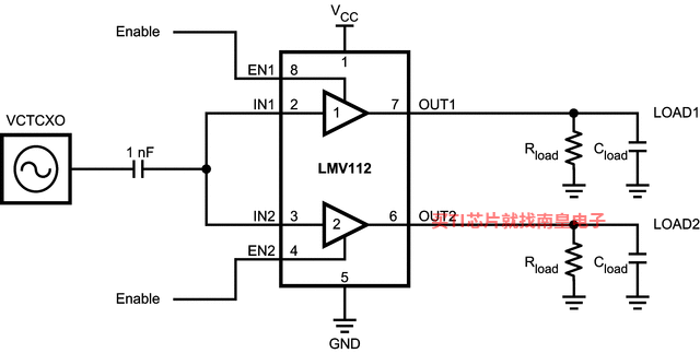
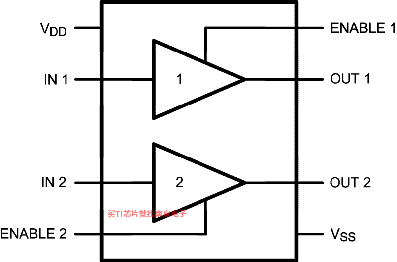
The LMV112 is a high speed dual clock buffer designed for portable communications and accurate multi-clock systems. The LMV112 integrates two 40 MHz low noise buffers which optimizes application and out performs large discrete solutions. This device enables superb system operation between the base band and the oscillator signal path while eliminating crosstalk.
Texas Instruments' unique technology and design deliver accuracy, capacitance and load resistance while increasing the drive capability of the device. The low power consumption makes the LMV112 perfect for battery applications.
The robust, independent, and flexible buffers are designed to provide the customer with the ability to manage complex clock signals in the latest wireless applications. The buffers deliver 110 V/μs internal slew rate with independent shutdown and duty cycle precision. The patented analog circuit drives capacitive loads beyond 20 pF. Texas Instruments' proven biasing technique has 1V centering, rail-to-rail input/output unity gain, and AC coupled convenient inputs. These integrated cells save space and require no external bias resistors. Texas Instruments' rapid recovery after disable optimizes performance and current consumption. The LMV112 offers individual enable pin controls and since there is no internal ground reference either single or split supply configurations offer additional system flexibility and power choices.
The LMV112 is a proven replacement for any discrete circuitry and simplifies board layout while minimizing related parasitic components.
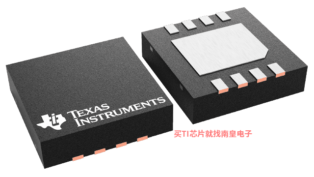
The LMV112 is produced in the small WSON package which offers high quality while minimizing its use of PCB space. Texas Instruments' advanced packaging offers direct PCB-IC evaluation via pin access.
- (Typical Values are: VSUPPLY = 2.7V and CL = 20pF, Unless Otherwise Specified.)
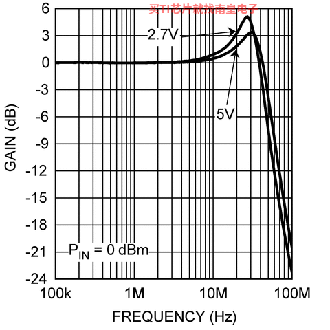
- Small Signal Bandwidth 40 MHz
- Supply Voltage Range 2.4V to 5V
- Slew Rate 110 V/μs
- Total Supply Current 1.6 mA
- Shutdown Current 59 μA
- Rail-to-Rail Input and Output
- Individual Buffer Enable Pins
- Rapid Ton Technology
- Crosstalk Rejection Circuitry
- 8-pin WSON, Pin Access Packaging
- Temperature Range ?40°C to 85°C
All trademarks are the property of their respective owners.
- Function
- Single-ended
- Output frequency (Max) (MHz)
- 40
- Number of outputs
- 2
- Output supply voltage (V)
- 2.5, 3.3, 5
- Core supply voltage (V)
- 2.5, 3.3, 5
- Features
- 1:2 fanout
- Operating temperature range (C)
- -40 to 85
- Rating
- Catalog
- Output type
- Rail-to-rail
- Input type
- Rail-to-rail
LMV112的完整型号有:LMV112SD/NOPB、LMV112SDX/NOPB,以下是这些产品的关键参数及官网采购报价:
LMV112SD/NOPB,工作温度:-40 to 85,封装:WSON (NGQ)-8,包装数量MPQ:1000个,MSL 等级/回流焊峰值温度:Level-1-260C-UNLIM,引脚镀层/焊球材料:SN,TI官网LMV112SD/NOPB的批量USD价格:.562(1000+)
LMV112SDX/NOPB,工作温度:-40 to 85,封装:WSON (NGQ)-8,包装数量MPQ:4500个,MSL 等级/回流焊峰值温度:Level-1-260C-UNLIM,引脚镀层/焊球材料:SN,TI官网LMV112SDX/NOPB的批量USD价格:.491(1000+)

PSPICE-FOR-TI ― 适用于 TI 设计和模拟工具的 PSpice
PSpice for TI 可提供帮助评估模拟电路功能的设计和仿真环境。此功能齐全的设计和仿真套件使用 Cadence 的模拟分析引擎。PSpice for TI 可免费使用,包括业内超大的模型库之一,涵盖我们的模拟和电源产品系列以及精选的模拟行为模型。借助?PSpice for TI 的设计和仿真环境及其内置的模型库,您可对复杂的混合信号设计进行仿真。创建完整的终端设备设计和原型解决方案,然后再进行布局和制造,可缩短产品上市时间并降低开发成本。
在?PSpice for TI 设计和仿真工具中,您可以搜索 TI (...)
TIDA-010057 ― Ultrasound smart probe power supply reference design
医疗成像领域的巨大技术进步和高集成度,特别是手持式超声波智能探头的出现,促使工程师开发出高效率、抗噪声的小尺寸电源解决方案。此参考设计阐述了端到端电源和数据解决方案,适用于我们采用 TX7332 发送芯片和 AFE5832LP 接收芯片的高性能 128 通道 Tx/64 通道 Rx 超声波智能探头。通过 5V USB Type-C™ 输入,电源树可生成用于发送的单级无变压器高压(高达 +/-80V,并且高度小于 5mm)以及用于 AFE 和 FPGA 的负载点低压。此设计可实现低噪声(纹波电压小于 10mV)高效电源轨并提高热性能(温升小于 (...)