- ЦЖФмі§ЙМЈєTI
- ІъЖ·Аа±рЈєЅУїЪ
- јјКхАаДїЈєUART
- №¦ДЬГиКцЈєѕЯУР 16 ЧЦЅЪ FIFOЎўКэѕЭЛЩВКёЯґп 5 ХЧО»/ГлµДЛ«В· UART
- µг»чХвАпґтїЄј°ПВФШNS16C2552µДјјКхОДµµЧКБП
- TIґъАнЗюµАЈ¬Мṩµ±ИХ·ў»хЎўСПёсµДЦКБї±кЧјЈ¬ВъЧгДъµДДї±кјЫёс

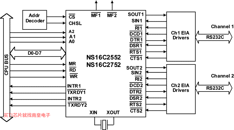
The NS16C2552 and NS16C2752 are dual channel Universal Asynchronous Receiver/Transmitter (DUART). The footprint and the functions are compatible to the PC16552D, while new features are added to the UART device. These features include low voltage support, 5V tolerant inputs, enhanced features, enhanced register set, and higher data rate.
The two serial channels are completely independent of each other, except for a common CPU interface and crystal input. On power-up both channels are functionally identical to the PC16552D. Each channel can operate with on-chip transmitter and receiver FIFO’s (in FIFO mode).
In the FIFO mode each channel is capable of buffering 16 bytes (for NS16C2552) or 64 bytes (for NS16C2752) of data in both the transmitter and receiver. The receiver FIFO also has additional 3 bits of error data per location. All FIFO control logic is on-chip to minimize system software overhead and maximize system efficiency.
To improve the CPU processing bandwidth, the data transfers between the DUART and the CPU can be done using DMA controller. Signaling for DMA transfers is done through two pins per channel (TXRDY and RXRDY). The RXRDYfunction is multiplexed on one pin with the OUT2 and BAUDOUT functions. The configuration is through Alternate Function Register.
The fundamental function of the UART is converting between parallel and serial data. Serial-to-parallel conversion is done on the UART receiver and parallel-to-serial conversion is done on the transmitter. The CPU can read the complete status of each channel at any time. Status information reported includes the type and condition of the transfer operations being performed by the DUART, as well as any error conditions (parity, overrun, framing, or break interrupt).
The NS16C2552 and NS16C2752 include one programmable baud rate generator for each channel. Each baud rate generator is capable of dividing the clock input by divisors of 1 to (216 - 1), and producing a 16X clock for driving the internal transmitter logic and for receiver sampling circuitry. The NS16C2552 and NS16C2752 have complete MODEM-control capability, and a processor-interrupt system. The interrupts can be programmed by the user to minimize the processing required to handle the communications link.
- Dual Independent UART
- Up to 5 Mbits/s Data Transfer Rate
- 2.97 V to 5.50 V Operational Vcc
- 5 V Tolerant I/Os in the Entire Supply Voltage Range
- Industrial Temperature: -40ЎгC to 85ЎгC
- Default Registers are Identical to the PC16552D
- NS16C2552/NS16C2752 is Pin-to-Pin Compatible to TI PC16552D, EXAR ST16C2552, XR16C2552, XR 16L2552, and Phillips SC16C2552B
- NS16C2752 is Compatible to EXAR XR16L2752, and Register Compatible to Phillips SC16C752
- Auto Hardware Flow Control (Auto-CTS, Auto-RTS)
- Auto Software Flow Control (Xon, Xoff, and Xon-any)
- Fully Programmable Character Length (5, 6, 7, or 8) with Even, Odd, or No Parity, Stop Bit
- Adds or Deletes Standard Asynchronous Communication Bits (Start, Stop, and Parity) to or from the Serial Data
- Independently Controlled and Prioritized Transmit and Receive Interrupts
- Complete Line Status Reporting Capabilities
- Line Break Generation and Detection
- Internal Diagnostic Capabilities
- Loopback Controls for Communications Link Fault Isolation
- Break, Parity, Overrun, Framing Error Detection
- Programmable Baud Generators Divide any Input Clock by 1 to (216 - 1) and Generate the 16 X clock
- IrDA v1.0 Wireless Infrared Encoder/Decoder
- DMA Operation (TXRDY/RXRDY)
- Concurrent Write to DUART Internal Register Channels 1 and 2
- Multi-Function Output Allows More Package Functions with Fewer I/O Pins
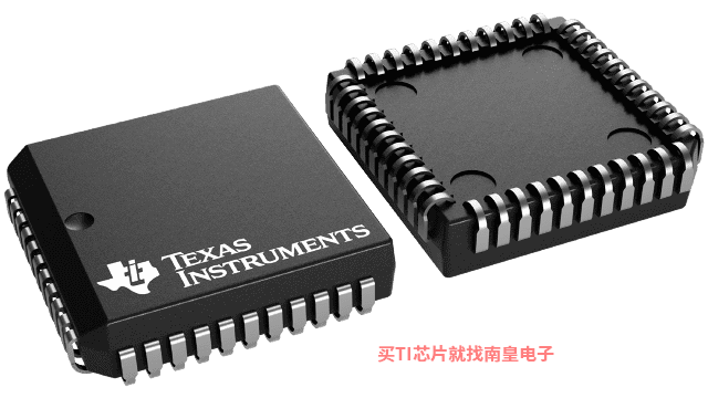
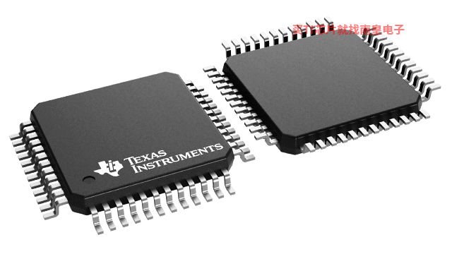
- 44-PLCC or 48-TQFP Package
All trademarks are the property of their respective owners.
- Number of channels (#)
- 2
- FIFOs (bytes)
- 16
- Rx FIFO trigger levels (#)
- 4
- Tx FIFO trigger levels (#)
- ЎЄ
- Programmable FIFO trigger levels
- No
- CPU interface
- X86
- Baud rate (max) at Vcc = 1.8 V & with 16X sampling (Mbps)
- ЎЄ
- Baud rate (max) at Vcc = 2.5 V & with 16X sampling (Mbps)
- ЎЄ
- Baud rate (max) at Vcc = 3.3 V & with 16X sampling (Mbps)
- 5
- Baud rate (max) at Vcc = 5.0 V & with 16X sampling (Mbps)
- 5
- Operating voltage (V)
- 3.3, 5
- Auto RTS/CTS
- Yes
- Rating
- Catalog
- Operating temperature range (C)
- -40 to 85
NS16C2552µДНкХыРНєЕУРЈєNS16C2552TVA/NOPBЎўNS16C2552TVS/NOPBЎўNS16C2552TVSX/NOPBЈ¬ТФПВКЗХвР©ІъЖ·µД№ШјьІОКэј°№ЩНшІЙ№є±ЁјЫЈє
NS16C2552TVA/NOPBЈ¬№¤ЧчОВ¶ИЈє-40 to 85Ј¬·вЧ°ЈєPLCC (FN)-44Ј¬°ьЧ°КэБїMPQЈє25ёцЈ¬MSL µИј¶/»ШБчєё·еЦµОВ¶ИЈєLevel-3-245C-168 HRЈ¬ТэЅЕ¶ЖІг/єёЗтІДБПЈєSNЈ¬TI№ЩНшNS16C2552TVA/NOPBµДЕъБїUSDјЫёсЈє5.244ЈЁ1000+Ј©
NS16C2552TVS/NOPBЈ¬№¤ЧчОВ¶ИЈє-40 to 85Ј¬·вЧ°ЈєTQFP (PFB)-48Ј¬°ьЧ°КэБїMPQЈє250ёцЈ¬MSL µИј¶/»ШБчєё·еЦµОВ¶ИЈєLevel-3-260C-168 HRЈ¬ТэЅЕ¶ЖІг/єёЗтІДБПЈєSNЈ¬TI№ЩНшNS16C2552TVS/NOPBµДЕъБїUSDјЫёсЈє5.72ЈЁ1000+Ј©
NS16C2552TVSX/NOPBЈ¬№¤ЧчОВ¶ИЈє-40 to 85Ј¬·вЧ°ЈєTQFP (PFB)-48Ј¬°ьЧ°КэБїMPQЈє1000ёцЈ¬MSL µИј¶/»ШБчєё·еЦµОВ¶ИЈєLevel-3-260C-168 HRЈ¬ТэЅЕ¶ЖІг/єёЗтІДБПЈєSNЈ¬TI№ЩНшNS16C2552TVSX/NOPBµДЕъБїUSDјЫёсЈє4.767ЈЁ1000+Ј©

PSPICE-FOR-TI ЎЄ ККУГУЪ TI ЙијЖєНДЈД⹤ѕЯµД PSpice
PSpice for TI їЙМṩ°пЦъЖА№АДЈДвµзВ·№¦ДЬµДЙијЖєН·ВХж»·ѕіЎЈґЛ№¦ДЬЖлИ«µДЙијЖєН·ВХжМЧјюК№УГ Cadence µДДЈДв·ЦОцТэЗжЎЈPSpice for TI їЙГв·СК№УГЈ¬°ьАЁТµДЪі¬ґуµДДЈРНївЦ®Т»Ј¬єёЗОТГЗµДДЈДвєНµзФґІъЖ·ПµБРТФј°ѕ«СЎµДДЈДвРРОЄДЈРНЎЈЅиЦъ?PSpice for TI µДЙијЖєН·ВХж»·ѕіј°ЖдДЪЦГµДДЈРНївЈ¬ДъїЙ¶ФёґФУµД»мєПРЕєЕЙијЖЅшРР·ВХжЎЈґґЅЁНкХыµДЦХ¶ЛЙи±ёЙијЖєНФРНЅвѕц·Ѕ°ёЈ¬И»єуФЩЅшРРІјѕЦєНЦЖФмЈ¬їЙЛх¶МІъЖ·ЙПКРК±јдІўЅµµНїЄ·ўіЙ±ѕЎЈ
ФЪ?PSpice for TI ЙијЖєН·ВХ湤ѕЯЦРЈ¬ДъїЙТФЛСЛч TI (...)
TINA-TI ЎЄ »щУЪ SPICE µДДЈДв·ВХжіМРт
TINA-TI МṩБЛ SPICE ЛщУРµДґ«НіЦ±БчЎўЛІМ¬єНЖµУт·ЦОцТФј°ёь¶аЎЈTINA ѕЯУР№г·єµДєуґ¦Ан№¦ДЬЈ¬ФКРнДъ°ґХХПЈНыµД·ЅКЅЙиЦГЅб№ыµДёсКЅЎЈРйДвТЗЖчФКРнДъСЎФсКдИлІЁРОЎўМЅХлµзВ·ЅЪµгµзС№єНІЁРОЎЈTINA µДФАнНјІ¶»с·ЗіЈЦ±№Ы - ХжХэµДЎ°їмЛЩИлГЕЎ±ЎЈTINA-TI °ІЧ°РиТЄґуФј 500MBЎЈЦ±ЅУ°ІЧ°Ј¬Из№ыПлР¶ФШТІєЬИЭТЧЎЈОТГЗПаРЕДъїП¶Ё»б°®І»КНКЦЎЈ
TINA КЗµВЦЭТЗЖч (TI) ЧЁУРµД DesignSoft ІъЖ·ЎЈёГГв·С°ж±ѕѕЯУРНкХыµД№¦ДЬЈ¬µ«І»Ц§іЦНкХы°ж TINA ЛщМṩµДДіР©ЖдЛы№¦ДЬЎЈ
ИзРи»сИЎїЙУГ TINA-TI ДЈРНµДНкХыБР±нЈ¬ЗлІОФДЈєSpiceRack - НкХыБР±н
РиТЄ HSpice (...)
