- 制造厂商:TI
- 产品类别:接口
- 技术类目:I2C IC - I2C 电平转换器、缓冲器和集线器
- 功能描述:2 位双向 2.3V 至 3.6V 400kHz I2C/SMBus 缓冲器
- 点击这里打开及下载PCA9515A的技术文档资料
- TI代理渠道,提供当日发货、严格的质量标准,满足您的目标价格

This dual bidirectional I2C buffer is operational at 2.3-V to 3.6-V VCC.
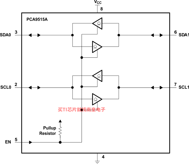
The PCA9515A is a BiCMOS integrated circuit intended for I2C bus and SMBus systems applications. The device contains two identical bidirectional open-drain buffer circuits that enable I2C and similar bus systems to be extended without degradation of system performance.
The PCA9515A buffers both the serial data (SDA) and serial clock (SCL) signals on the I2C bus, while retaining all the operating modes and features of the I2C system. This enables two buses of 400-pF bus capacitance to be connected in an I2C application.
The I2C bus capacitance limit of 400 pF restricts the number of devices and bus length. Using the PCA9515A enables the system designer to isolate two halves of a bus, accommodating more I2C devices or longer trace lengths.
The PCA9515A has an active-high enable (EN) input with an internal pullup, which allows the user to select when the repeater is active. This can be used to isolate a badly behaved slave on power-up reset. It never should change state during an I2C operation, because disabling during a bus operation hangs the bus, and enabling part way through a bus cycle could confuse the I2C parts being enabled. The EN input should change state only when the global bus and the repeater port are in an idle state, to prevent system failures.
The PCA9515A also can be used to run two buses: one at 5-V interface levels and the other at 3.3-V interface levels, or one at 400-kHz operating frequency and the other at 100-kHz operating frequency. If the two buses are operating at different frequencies, the 100-kHz bus must be isolated when the 400-kHz operation of the other bus is required. If the master is running at 400 kHz, the maximum system operating frequency may be less than 400 kHz, because of the delays that are added by the repeater.
The PCA9515A does not support clock stretching across the repeater.
The output low levels for each internal buffer are approximately 0.5 V, but the input voltage of each internal buffer must be 70 mV or more below the output low level, when the output internally is driven low. This prevents a lockup condition from occurring when the input low condition is released.
Two or more PCA9515A devices cannot be used in series. The PCA9515A design does not allow this configuration. Because there is no direction pin, slightly different valid low-voltage levels are used to avoid lockup conditions between the input and the output of each repeater. A valid low applied at the input of a PCA9515A is propagated as a buffered low with a slightly higher value on the enabled outputs. When this buffered low is applied to another PCA9515A-type device in series, the second device does not recognize it as a valid low and does not propagate it as a buffered low again.
The device contains a power-up control circuit that sets an internal latch to prevent the output circuits from becoming active until VCC is at a valid level (VCC = 2.3 V).
As with the standard I2C system, pullup resistors are required to provide the logic high levels on the buffered bus. The PCA9515A has standard open-collector configuration of the I2C bus. The size of these pullup resistors depends on the system, but each side of the repeater must have a pullup resistor. The device is designed to work with Standard Mode and Fast Mode I2C devices in addition to SMBus devices. Standard Mode I2C devices only specify 3 mA in a generic I2C system where Standard Mode devices and multiple masters are possible. Under certain conditions, high termination currents can be used.
- Two-Channel Bidirectional Buffers
- I2C Bus and SMBus Compatible
- Active-High Repeater-Enable Input
- Open-Drain I2C I/O
- 5.5-V Tolerant I2C I/O and Enable Input Support Mixed-Mode Signal Operation
- Lockup-Free Operation
- Accommodates Standard Mode and Fast Mode I2C Devices and Multiple Masters
- Powered-Off High-Impedance I2C Pins
- Latch-Up Performance Exceeds 100 mA Per JESD 78, Class II
- ESD Protection Exceeds JESD 22
- 2000-V Human-Body Model (A114-A)
- 200-V Machine Model (A115-A)
- 1000-V Charged-Device Model (C101)
All trademarks are the property of their respective owners.
- Features
- Buffer
- Frequency (Max) (kHz)
- 400
- VCCA (Min) (V)
- 2.3
- VCCA (Max) (V)
- 3.6
- VCCB (Min) (V)
- 2.3
- VCCB (Max) (V)
- 3.6
- Supply restrictions
- VCC Single Supply
- Rating
- Catalog
- Operating temperature range (C)
- -40 to 85
PCA9515A的完整型号有:PCA9515AD、PCA9515ADR、PCA9515ADRGR、PCA9515ADT、PCA9515APW、PCA9515APWR、PCA9515APWT、PCA9515ADGKR、PCA9515ADGKT,以下是这些产品的关键参数及官网采购报价:
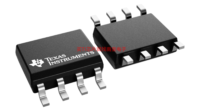
PCA9515AD,工作温度:-40 to 85,封装:SOIC (D)-8,包装数量MPQ:75个,MSL 等级/回流焊峰值温度:Level-1-260C-UNLIM,引脚镀层/焊球材料:NIPDAU,TI官网PCA9515AD的批量USD价格:.872(1000+)
PCA9515ADR,工作温度:-40 to 85,封装:SOIC (D)-8,包装数量MPQ:2500个,MSL 等级/回流焊峰值温度:Level-1-260C-UNLIM,引脚镀层/焊球材料:NIPDAU,TI官网PCA9515ADR的批量USD价格:.743(1000+)
PCA9515ADRGR,工作温度:-40 to 85,封装:SON (DRG)-8,包装数量MPQ:3000个,MSL 等级/回流焊峰值温度:Level-2-260C-1 YEAR,引脚镀层/焊球材料:NIPDAU,TI官网PCA9515ADRGR的批量USD价格:.743(1000+)
PCA9515ADT,工作温度:-40 to 85,封装:SOIC (D)-8,包装数量MPQ:250个,MSL 等级/回流焊峰值温度:Level-1-260C-UNLIM,引脚镀层/焊球材料:NIPDAU,TI官网PCA9515ADT的批量USD价格:.872(1000+)
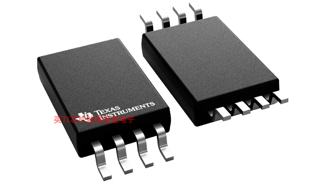
PCA9515APW,工作温度:-40 to 85,封装:TSSOP (PW)-8,包装数量MPQ:150个,MSL 等级/回流焊峰值温度:Level-1-260C-UNLIM,引脚镀层/焊球材料:NIPDAU,TI官网PCA9515APW的批量USD价格:.872(1000+)
PCA9515APWR,工作温度:-40 to 85,封装:TSSOP (PW)-8,包装数量MPQ:2000个,MSL 等级/回流焊峰值温度:Level-1-260C-UNLIM,引脚镀层/焊球材料:NIPDAU,TI官网PCA9515APWR的批量USD价格:.743(1000+)
PCA9515APWT,工作温度:-40 to 85,封装:TSSOP (PW)-8,包装数量MPQ:250个,MSL 等级/回流焊峰值温度:Level-1-260C-UNLIM,引脚镀层/焊球材料:NIPDAU,TI官网PCA9515APWT的批量USD价格:.872(1000+)
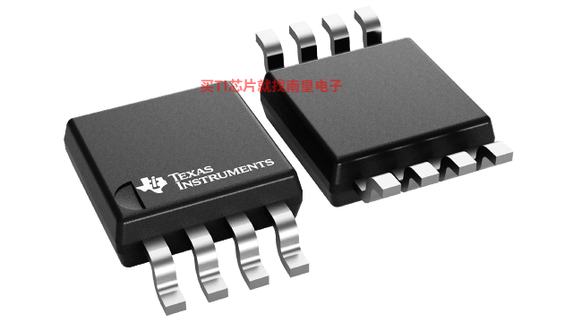
PCA9515ADGKR,工作温度:-40 to 85,封装:VSSOP (DGK)-8,包装数量MPQ:2500个,MSL 等级/回流焊峰值温度:Level-1-260C-UNLIM,引脚镀层/焊球材料:NIPDAU,TI官网PCA9515ADGKR的批量USD价格:.743(1000+)
PCA9515ADGKT,工作温度:-40 to 85,封装:VSSOP (DGK)-8,包装数量MPQ:250个,MSL 等级/回流焊峰值温度:Level-1-260C-UNLIM,引脚镀层/焊球材料:NIPDAU,TI官网PCA9515ADGKT的批量USD价格:.872(1000+)

HSPICE Model for PCA9515A
PSpice for TI 可提供帮助评估模拟电路功能的设计和仿真环境。此功能齐全的设计和仿真套件使用 Cadence 的模拟分析引擎。PSpice for TI 可免费使用,包括业内超大的模型库之一,涵盖我们的模拟和电源产品系列以及精选的模拟行为模型。借助?PSpice for TI 的设计和仿真环境及其内置的模型库,您可对复杂的混合信号设计进行仿真。创建完整的终端设备设计和原型解决方案,然后再进行布局和制造,可缩短产品上市时间并降低开发成本。
在?PSpice for TI 设计和仿真工具中,您可以搜索 TI (...)
TINA-TI ― 基于 SPICE 的模拟仿真程序
TINA-TI 提供了 SPICE 所有的传统直流、瞬态和频域分析以及更多。TINA 具有广泛的后处理功能,允许您按照希望的方式设置结果的格式。虚拟仪器允许您选择输入波形、探针电路节点电压和波形。TINA 的原理图捕获非常直观 - 真正的“快速入门”。TINA-TI 安装需要大约 500MB。直接安装,如果想卸载也很容易。我们相信您肯定会爱不释手。
TINA 是德州仪器 (TI) 专有的 DesignSoft 产品。该免费版本具有完整的功能,但不支持完整版 TINA 所提供的某些其他功能。
如需获取可用 TINA-TI 模型的完整列表,请参阅:SpiceRack - 完整列表
需要 HSpice (...)
I2C-DESIGNER ― I2C designer tool
利用 I2C 设计器工具,可快速解决基于 I2C 设计中寻址、电压电平和频率方面的冲突。输入主输入端和从输入端,以自动生成 I2C 树活轻松构建自定义解决方案。此工具可在调试缺失确认、选择上拉电阻器和满足 I2C 总线最大容性负载方面提供指导,从而帮助设计人员节省时间并遵循 I2C 标准。