- 制造厂商:TI
- 产品类别:接口
- 技术类目:其他接口
- 功能描述:具有 IEEE 1149.1 测试访问的 20 至 66MHz 10 位解串器
- 点击这里打开及下载SCAN921224的技术文档资料
- TI代理渠道,提供当日发货、严格的质量标准,满足您的目标价格

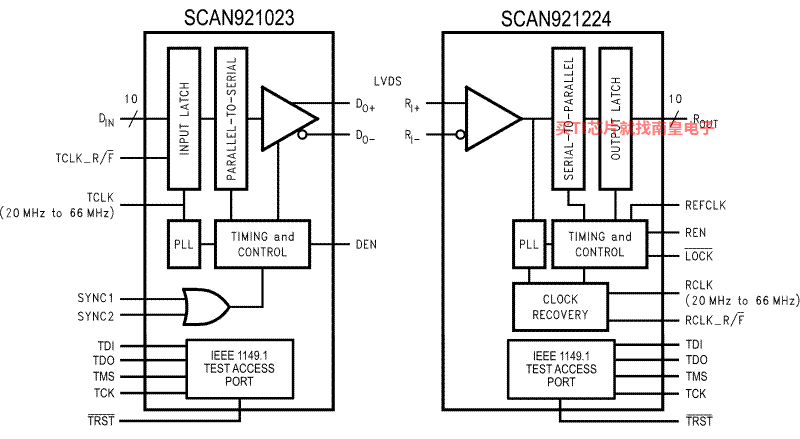
The SCAN921023 transforms a 10-bit wide parallel LVCMOS/LVTTL data bus into a single high speed Bus LVDS serial data stream with embedded clock. The SCAN921224 receives the Bus LVDS serial data stream and transforms it back into a 10-bit wide parallel data bus and recovers parallel clock. Both devices are compliant with IEEE 1149.1 Standard Test Access Port and Boundary Scan Architecture with the incorporation of the defined boundary-scan test logic and test access port consisting of Test Data Input (TDI), Test Data Out (TDO), Test Mode Select (TMS), Test Clock (TCK), and the optional Test Reset (TRST). IEEE 1149.1 features provide the designer or test engineer access to the backplane or cable interconnects and the ability to verify differential signal integrity to enhance their system test strategy. The pair of devices also features an at-speed BIST mode which allows the interconnects between the Serializer and Deserializer to be verified at-speed.
The SCAN921023 transmits data over backplanes or cable. The single differential pair data path makes PCB design easier. In addition, the reduced cable, PCB trace count, and connector size tremendously reduce cost. Since one output transmits clock and data bits serially, it eliminates clock-to-data and data-to-data skew. The powerdown pin saves power by reducing supply current when not using either device. Upon power up of the Serializer, you can choose to activate synchronization mode or allow the Deserializer to use the synchronization-to-random-data feature. By using the synchronization mode, the Deserializer will establish lock to a signal within specified lock times. In addition, the embedded clock ensures a transition on the bus every 12-bit cycle. This eliminates transmission errors due to charged cable conditions. Furthermore, you may put the SCAN921023 output pins into TRI-STATE to achieve a high impedance state. The PLL can lock to frequencies between 20 MHz and 66 MHz.
- IEEE 1149.1 (JTAG) Compliant and At-Speed BIST Test Mode
- Clock Recovery From PLL Lock to Random Data Patterns
- Ensured Transition Every Data Transfer Cycle
- Chipset (Tx + Rx) Power Consumption < 500 mW (typ) @ 66 MHz
- Single Differential Pair Eliminates Multi-Channel Skew
- Flow-Through Pinout for Easy PCB Layout
- 660 Mbps Serial Bus LVDS Data Rate (at 66 MHz Clock)
- 10-bit Parallel Interface for 1 Byte Data Plus 2 Control Bits
- Synchronization Mode and LOCK Indicator
- Programmable Edge Trigger on Clock
- High Impedance on Receiver Inputs when Power is Off
- Bus LVDS Serial Output Rated for 27? Load
- Small 49-Lead NFBGA Package
All trademarks are the property of their respective owners.
- Operating temperature range (C)
- -40 to 85
SCAN921224的完整型号有:SCAN921224SLC/NOPB、SCAN921224SLC,以下是这些产品的关键参数及官网采购报价:
SCAN921224SLC/NOPB,工作温度:-40 to 85,封装:NFBGA (NZA)-49,包装数量MPQ:416个,MSL 等级/回流焊峰值温度:Level-4-260C-72 HR,引脚镀层/焊球材料:SNAGCU,TI官网SCAN921224SLC/NOPB的批量USD价格:4.879(1000+)
SCAN921224SLC,工作温度:-40 to 85,封装:NFBGA (NZA)-49,包装数量MPQ:416个,MSL 等级/回流焊峰值温度:Level-3-235C-168 HR,引脚镀层/焊球材料:SNPB,TI官网SCAN921224SLC的批量USD价格:6.653(1000+)

PSPICE-FOR-TI — 适用于 TI 设计和模拟工具的 PSpice
PSpice for TI 可提供帮助评估模拟电路功能的设计和仿真环境。此功能齐全的设计和仿真套件使用 Cadence 的模拟分析引擎。PSpice for TI 可免费使用,包括业内超大的模型库之一,涵盖我们的模拟和电源产品系列以及精选的模拟行为模型。借助?PSpice for TI 的设计和仿真环境及其内置的模型库,您可对复杂的混合信号设计进行仿真。创建完整的终端设备设计和原型解决方案,然后再进行布局和制造,可缩短产品上市时间并降低开发成本。
在?PSpice for TI 设计和仿真工具中,您可以搜索 TI (...)
TINA-TI — 基于 SPICE 的模拟仿真程序
TINA-TI 提供了 SPICE 所有的传统直流、瞬态和频域分析以及更多。TINA 具有广泛的后处理功能,允许您按照希望的方式设置结果的格式。虚拟仪器允许您选择输入波形、探针电路节点电压和波形。TINA 的原理图捕获非常直观 - 真正的“快速入门”。TINA-TI 安装需要大约 500MB。直接安装,如果想卸载也很容易。我们相信您肯定会爱不释手。
TINA 是德州仪器 (TI) 专有的 DesignSoft 产品。该免费版本具有完整的功能,但不支持完整版 TINA 所提供的某些其他功能。
如需获取可用 TINA-TI 模型的完整列表,请参阅:SpiceRack - 完整列表
需要 HSpice (...)


