- 制造厂商:TI
- 产品类别:接口
- 技术类目:LVDS、M-LVDS 和 PECL IC
- 功能描述:具有边界扫描功能的 9 通道总线 LVDS 收发器
- 点击这里打开及下载SCAN92LV090的技术文档资料
- TI代理渠道,提供当日发货、严格的质量标准,满足您的目标价格

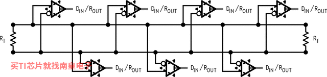
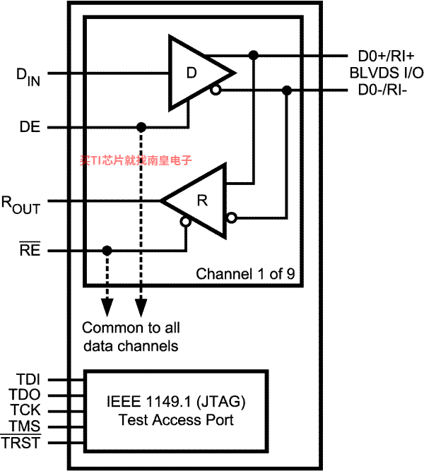
The SCAN92LV090A is one in a series of Bus LVDS transceivers designed specifically for the high speed, low power proprietary backplane or cable interfaces. The device operates from a single 3.3V power supply and includes nine differential line drivers and nine receivers. To minimize bus loading, the driver outputs and receiver inputs are internally connected. The separate I/O of the logic side allows for loop back support. The device also features a flow through pin out which allows easy PCB routing for short stubs between its pins and the connector.
The driver translates 3V TTL levels (single-ended) to differential Bus LVDS (BLVDS) output levels. This allows for high speed operation, while consuming minimal power with reduced EMI. In addition, the differential signaling provides common mode noise rejection of ±1V.
The receiver threshold is less than ±100 mV over a ±1V common mode range and translates the differential Bus LVDS to standard (TTL/CMOS) levels.
This device is compliant with IEEE 1149.1 Standard Test Access Port and Boundary Scan Architecture with the incorporation of the defined boundary-scan test logic and test access port consisting of Test Data Input (TDI), Test Data Out (TDO), Test Mode Select (TMS), Test Clock (TCK), and the optional Test Reset (TRST).
- IEEE 1149.1 (JTAG) Compliant
- Bus LVDS Signaling
- Low Power CMOS Design
- High Signaling Rate Capability (Above 100 Mbps)
- 0.1V to 2.3V Common Mode Range for VID = 200mV
- ±100 mV Receiver Sensitivity
- Supports Open and Terminated Failsafe on Port Pins
- 3.3V Operation
- Glitch Free Power Up/Down (Driver & Receiver Disabled)
- Light Bus Loading (5 pF Typical) per Bus LVDS Load
- Designed for Double Termination Applications
- Balanced Output Impedance
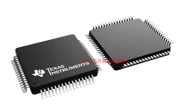
- Product Offered in 64 Pin LQFP Package and NFBGA Package
- High Impedance Bus Pins on Power Off (VCC = 0V)
All trademarks are the property of their respective owners.
- Function
- Transceiver
- Protocols
- JTAG IEEE1149.1, BLVDS
- Number of transmitters
- 9
- Number of receivers
- 9
- Supply voltage (V)
- 3.3
- Signaling rate (Mbps)
- 100
- Input signal
- LVDS, BLVDS, LVTTL, LVCMOS
- Output signal
- BLVDS
- Rating
- Catalog
- Operating temperature range (C)
- -40 to 85
SCAN92LV090的完整型号有:SCAN92LV090SLC/NOPB、SCAN92LV090VEH/NOPB、SCAN92LV090SLC,以下是这些产品的关键参数及官网采购报价:
SCAN92LV090SLC/NOPB,工作温度:-40 to 85,封装:NFBGA (NZC)-64,包装数量MPQ:360个,MSL 等级/回流焊峰值温度:Level-4-260C-72 HR,引脚镀层/焊球材料:SNAGCU,TI官网SCAN92LV090SLC/NOPB的批量USD价格:4.646(1000+)
SCAN92LV090VEH/NOPB,工作温度:-40 to 85,封装:LQFP (PM)-64,包装数量MPQ:160个,MSL 等级/回流焊峰值温度:Level-3-260C-168 HR,引脚镀层/焊球材料:SN,TI官网SCAN92LV090VEH/NOPB的批量USD价格:5.491(1000+)
SCAN92LV090SLC,工作温度:-40 to 85,封装:NFBGA (NZC)-64,包装数量MPQ:360个,MSL 等级/回流焊峰值温度:Level-3-235C-168 HR,引脚镀层/焊球材料:SNPB,TI官网SCAN92LV090SLC的批量USD价格:6.336(1000+)

PSPICE-FOR-TI ― 适用于 TI 设计和模拟工具的 PSpice
PSpice for TI 可提供帮助评估模拟电路功能的设计和仿真环境。此功能齐全的设计和仿真套件使用 Cadence 的模拟分析引擎。PSpice for TI 可免费使用,包括业内超大的模型库之一,涵盖我们的模拟和电源产品系列以及精选的模拟行为模型。借助?PSpice for TI 的设计和仿真环境及其内置的模型库,您可对复杂的混合信号设计进行仿真。创建完整的终端设备设计和原型解决方案,然后再进行布局和制造,可缩短产品上市时间并降低开发成本。
在?PSpice for TI 设计和仿真工具中,您可以搜索 TI (...)
TINA-TI ― 基于 SPICE 的模拟仿真程序
TINA-TI 提供了 SPICE 所有的传统直流、瞬态和频域分析以及更多。TINA 具有广泛的后处理功能,允许您按照希望的方式设置结果的格式。虚拟仪器允许您选择输入波形、探针电路节点电压和波形。TINA 的原理图捕获非常直观 - 真正的“快速入门”。TINA-TI 安装需要大约 500MB。直接安装,如果想卸载也很容易。我们相信您肯定会爱不释手。
TINA 是德州仪器 (TI) 专有的 DesignSoft 产品。该免费版本具有完整的功能,但不支持完整版 TINA 所提供的某些其他功能。
如需获取可用 TINA-TI 模型的完整列表,请参阅:SpiceRack - 完整列表
需要 HSpice (...)