- жЦдьГЇЩЬЃКTI
- ВњЦЗРрБ№ЃКЮЂПижЦЦї (MCU) КЭДІРэЦї
- ММЪѕРрФПЃКДІРэЦї - Ъ§зжаХКХДІРэЦї (DSP)
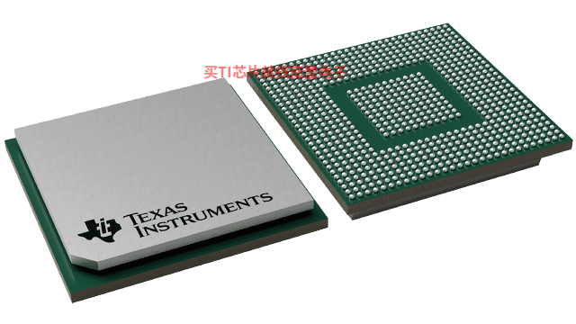
- ЙІФмУшЪіЃКИпПЩППадВњЦЗ 6 КЫ C6472 ЖЈЕу DSP
- ЕуЛїетРяДђПЊМАЯТдиSM320C6472-HIRELЕФММЪѕЮФЕЕзЪСЯ
- TIДњРэЧўЕРЃЌЬсЙЉЕБШеЗЂЛѕЁЂбЯИёЕФжЪСПБъзМЃЌТњзуФњЕФФПБъМлИё

The SM320C6472 device is a Texas Instruments next-generation fixed-point digital signal processor (DSP) targeting high-performance computing applications, including high-end industrial, mission-critical, high-end image and video, communication, media gateways, and remote access servers. This device was designed with these applications in mind. A common key requirement of these applications is the availability of large on-chip memories to handle vast amounts of data during processing. With 768K-Byte of shared RAM and 608K-Byte local L2 RAM per C64x+ Megamodule, the SM320C6472 device can eliminate the need for external memory, thereby reducing system power dissipation and system cost and optimizing board density.
The SM320C6472 device has six optimized TMS320C64x+™ megamodules, which combine high performance with the lowest power dissipation per port. The TMS320C6472 device includes three different speeds: 500 MHz, 625 MHz, and 700 MHz. The C64x+ megamodules are the highest-performance fixed-point DSP generation in the TMS320C6000™ DSP platform. The C64x+ megamodule is based on the third-generation high-performance, advanced VelociTI™ very-long-instruction-word (VLIW) architecture developed by Texas Instruments (TI), making devices like SM320C6472 an excellent choice for applications including video and telecom infrastructure, imaging/medical, and wireless infrastructure (WI). The C64x+™ devices are upward code-compatible from previous devices that are part of the C6000™ DSP platform.
The C64x+ megamodule core employs eight functional units, two register files, and two data paths. Like the earlier C6000 devices, two of these eight functional units are multipliers or .M units. Each C64x+ megamodule core .M unit doubles the multiply throughput versus the C64x core by performing four 16-bit x 16-bit multiply-accumulates (MACs) every clock cycle. Thus, eight 16-bit x 16-bit MACs can be executed every cycle on the C64x+ core. At a 500-MHz clock rate, this means 4000 16-bit MMACs can occur every second. Moreover, each multiplier on the C64x+ megamodule core can compute one 32-bit x 32-bit MAC or four 8-bit x 8-bit MACs every clock cycle.
The C64x+ megamodule integrates a large amount of on-chip memory organized as a two-level memory system. The level-1 (L1) program and data memories on this C64x+ megamodule are 32KB each. This memory can be configured as mapped RAM, cache, or some combination of the two. When configured as cache, L1 program (L1P) is a direct mapped cache where as L1 data (L1D) is a two-way set associative cache. The level 2 (L2) memory is shared between program and data space and is 608K-Byte in size. L2 memory can also be configured as mapped RAM, cache, or some combination of the two. The C64x+ megamodule also has a 32-bit peripheral configuration (CFG) port, an internal DMA (IDMA) controller, a system component with reset/boot control, interrupt/exception control, a power-down control, and a free-running 32-bit timer for time stamp.
The peripheral set includes: three Telecom Serial Interface Port (TSIPs); an 16/8 bit Universal Test and Operations PHY Interface for Asynchronous Transfer Mode (ATM) Slave [UTOPIA Slave] port; two 10/100/1000 Ethernet media access controllers (EMACs), which provide an efficient interface between the C6472 DSP core processor and the network; a management data input/output (MDIO) module (shared by both EMACs) that continuously polls all 32 MDIO addresses in order to enumerate all PHY devices in the system; a Serial RapidIO® with two 1x lanes and support for packet forwarding; a 32-bit DDR2 SDRAM interface; 12 64-bit general-purpose timers; an inter-integrated circuit bus module (I2C); 16 general-purpose input/output ports (GPIO) with programmable interrupt/event generation modes; and a 16-bit multiplexed host-port interface (HPI16).
The C6472 device has a complete set of development tools which includes: a C compiler, an assembly optimizer to simplify programming and scheduling, and a Windows® debugger interface for visibility into source code execution.
- Six On-Chip TMS320C64x+ Megamodules
- Endianess: Little Endian, Big Endian
- C64x+ Megamodule Main Features:
- High-Performance, Fixed-Point TMS320C64x+ DSP
- 500/625/700 MHz
- Eight 32-Bit Instructions/Cycle
- 4000 MIPS/MMACS (16-Bits) at 500 MHz
- Dedicated SPLOOP Instruction
- Compact Instructions (16-Bit)
- Instruction Set Enhancements
- Exception Handling
- L1/L2 Memory Architecture:
- 256K-Bit (32K-Byte) L1P Program RAM/Cache [Direct Mapped, Flexible Allocation]
- 256K-Bit (32K-Byte) L1D RAM/Cache [2-Way Set-Associative, Flexible Allocation]
- 4.75M-Bit (608K-Byte) L2 Unified Mapped RAM/Cache [4-Way Set-Associative, Flexible Allocation]
- L1P Memory Controller
- L1D Memory Controller
- L2 Memory Controller
- Time Stamp Counter
- One 64-Bit General-Purpose/Watchdog Timer
- Shared Peripherals and Interfaces
- EDMA Controller (64 Independent Channels)
- Shared Memory Architecture
- Shared L2 Memory Controller
- 768K-Byte of RAM
- Boot ROM
- Three Telecom Serial Interface Ports (TSIPs)
- Each TSIP is 8 Links of 8 Mbps per Direction
- 32-Bit DDR2 Memory Controller (DDR2-533 SDRAM)
- 256 M-Byte ЁС 2 Addressable Memory Space
- Two 1x Serial RapidIO? Links, v1.2 Compliant
- 1.25-, 2.5-, 3.125-Gbps Link Rates
- Message Passing, DirectIO Support, Error Management Extensions, and Congestion Control
- IEEE 1149.6 Compliant I/Os
- UTOPIA
- UTOPIA Level 2 Slave ATM Controller
- 8/16-Bit Transmit and Receive Operations up to 50 MHz per Direction
- User-Defined Cell Format up to 64 Bytes
- Two 10/100/1000 Mb/s Ethernet MACs (EMACs)
- Both EMACs are IEEE 802.3 Compliant
- EMAC0 Supports:
- MII, RMII, SS-SMII, GMII, and RGMII
- 8 Independent Transmit (TX) Channels
- 8 Independent Receive (RX) Channels
- EMAC1 Supports:
- RMII, SS-SMII and RGMII
- 8 Independent Transmit (TX) Channels
- 8 Independent Receive (RX) Channels
- Both EMACs (EMAC0 and EMAC1) Share MDIO Interface
- 16-Bit Host-Port Interface (HPI)
- One Inter-Integrated Circuit (I2C) Bus
- Six Shared 64-Bit General-Purpose Timers
- System PLL and PLL Controller
- Secondary PLL and PLL Controller, Dedicated to EMAC
- Third PLL and PLL Controller Dedicated to DDR2 Memory Controller
- 16 General-Purpose I/O (GPIO) Pins
- IEEE-1149.1 (JTAG?) Boundary-Scan-Compatible
- 737-Pin Ball Gird Array (BGA) Package (ZTZ/GTZ Suffix), 0.8-mm Ball Pitch
- 0.09-ІЬm/7-Level Cu Metal Process (CMOS)
- 3.3-, 1.8-, 1.5-, 1.2-V I/O Supplies
- 1.0-/1.1-, 1.2-V Core Supplies
- Commercial Temperature [0ЁуC to 85ЁуC]
- Extended Temperature [ЈC40ЁуC to 100ЁуC]
- Only 625-MHz Device Offered in GTZ Package
- DSP
- 6 C64x+
- DSP MHz (Max)
- 700
- CPU
- 32-/64-bit
- Operating system
- DSP/BIOS
- Ethernet MAC
- 10/100/1000
- Rating
- Military
- Operating temperature range (C)
- -40 to 100
SM320C6472-HIRELЕФЭъећаЭКХгаЃКSM320C6472EGTZA6ЃЌвдЯТЪЧетаЉВњЦЗЕФЙиМќВЮЪ§МАЙйЭјВЩЙКБЈМлЃК
SM320C6472EGTZA6ЃЌЙЄзїЮТЖШЃК-40 to 100ЃЌЗтзАЃКFCBGA (GTZ)-737ЃЌАќзАЪ§СПMPQЃК44ИіЃЌMSL ЕШМЖ/ЛиСїКИЗхжЕЮТЖШЃКLevel-4-220C-72 HRЃЌв§НХЖЦВу/КИЧђВФСЯЃКSNPBЃЌTIЙйЭјSM320C6472EGTZA6ЕФХњСПUSDМлИёЃК282.241ЃЈ1000+ЃЉ

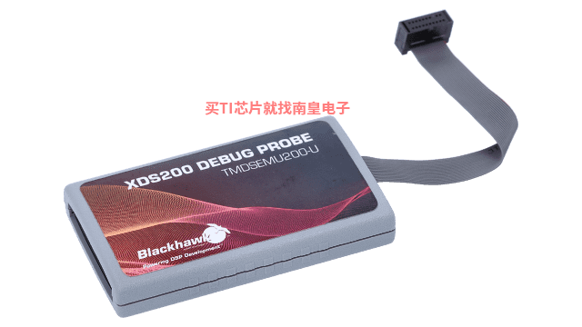
TMDSEMU200-U ЁЊ Spectrum Digital XDS200 USB ЗТецЦї
Spectrum Digital XDS200 ЪЧзюаТ XDS200 ЯЕСа TI ДІРэЦїЕїЪдЬНеыЃЈЗТецЦїЃЉЕФЪзИіФЃаЭЁЃXDS200 ЯЕСагЕгаГЌЕЭГЩБО XDS100 гыИпадФм XDS560v2 жЎМфЕФЕЭГЩБОгыИпадФмЕФЭъУРЦНКтЁЃДЫЭтЃЌЖдгкДјгаЧЖШыЪНЛКГхИњзйЦї (ETB) ЕФЫљга ARM КЭ DSP ДІРэЦїЃЌЫљга XDS ЕїЪдЬНеыОљжЇГжФкКЫКЭЯЕЭГИњзйЁЃ
Spectrum Digital XDS200 ЭЈЙ§ TI 20 в§НХСЌНгЦїЃЈДјгаЪЪКЯ TI 14 в§НХЁЂTI 10 в§НХКЭ ARM 20 в§НХЕФЖрИіЪЪХфЦїЃЉСЌНгЕНФПБъАхЃЌЖјЭЈЙ§ USB2.0 ИпЫйСЌНг (480Mbps) СЌНгЕНжїЛњ PCЁЃвЊдкжїЛњ (...)
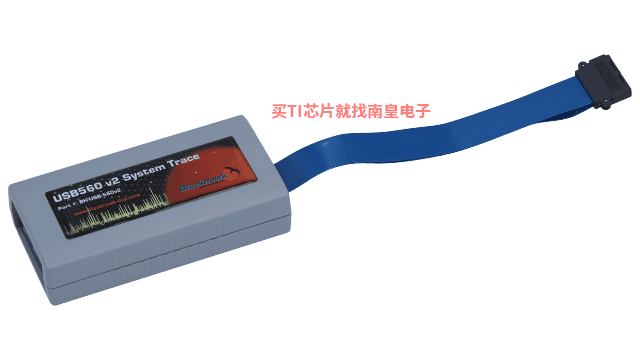
TMDSEMU560V2STM-U ЁЊ Blackhawk XDS560v2 ЯЕЭГИњзй USB ЗТецЦї
XDS560v2 System Trace ЪЧ XDS560v2 ЯЕСаИпадФм TI ДІРэЦїЕїЪдЬНеыЃЈЗТецЦїЃЉЕФЕквЛжжаЭКХЁЃXDS560v2 ЪЧ XDS ЯЕСаЕїЪдЬНеыжаадФмзюИпЕФвЛПюЃЌЭЌЪБжЇГжДЋЭГ JTAG БъзМ (IEEE1149.1) КЭ cJTAG (IEEE1149.7)ЁЃ
XDS560v2 System Trace дкЦфОоДѓЕФЭтВПДцДЂЦїЛКГхЧјжаМгШыСЫЯЕЭГв§НХИњзйЁЃетжжЭтВПДцДЂЦїЛКГхЧјЪЪгУгкжИЖЈЕФ TI ЦїМўЃЌЭЈЙ§ВЖЛёЯрЙиЦїМўМЖаХЯЂЃЌЛёЕУзМШЗЕФзмЯпадФмЛюЖЏКЭЭЬЭТСПЃЌВЂЖдФкКЫКЭЭтЩшНјааЕчдДЙмРэЁЃДЫЭтЃЌЖдгкДјгаЧЖШыЪНЛКГхИњзйЦї (ETB) ЕФЫљга ARM КЭ DSP ДІРэЦїЃЌЫљга XDS (...)
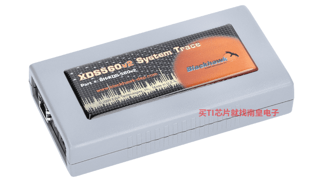
TMDSEMU560V2STM-UE ЁЊ Spectrum Digital XDS560v2 ЯЕЭГИњзй USB КЭвдЬЋЭј
XDS560v2 System Trace ЪЧ XDS560v2 ЯЕСаИпадФм TI ДІРэЦїЕїЪдЬНеыЃЈЗТецЦїЃЉЕФЕквЛжжаЭКХЁЃXDS560v2 ЪЧ XDS ЯЕСаЕїЪдЬНеыжаадФмзюИпЕФвЛПюЃЌЭЌЪБжЇГжДЋЭГ JTAG БъзМ (IEEE1149.1) КЭ cJTAG (IEEE1149.7)ЁЃ
XDS560v2 System Trace дкЦфОоДѓЕФЭтВПДцДЂЦїЛКГхЧјжаМгШыСЫЯЕЭГв§НХИњзйЁЃетжжЭтВПДцДЂЦїЛКГхЧјЪЪгУгкжИЖЈЕФ TI ЦїМўЃЌЭЈЙ§ВЖЛёЯрЙиЦїМўМЖаХЯЂЃЌЛёЕУзМШЗЕФзмЯпадФмЛюЖЏКЭЭЬЭТСПЃЌВЂЖдФкКЫКЭЭтЩшНјааЕчдДЙмРэЁЃДЫЭтЃЌЖдгкДјгаЧЖШыЪНЛКГхИњзйЦї (ETB) ЕФЫљга ARM КЭ DSP ДІРэЦїЃЌЫљга XDS (...)
FAXLIB — гУгк C66xЁЂC64x+ КЭ C55x ДІРэЦїЕФДЋецПт (FAXLIB)
TMS320C6000 Digital Signal Processor Library (DSPLIB) is a platform-optimized DSP function library for C programmers. It includes C-callable, general-purpose signal-processing routines that are typically used in computationally intensive real-time applications. With these routines, higher (...)CCSTUDIO-KEYSTONE ЁЊ ЪЪгУгкЖрКЫДІРэЦїЕФ Code Composer Studio (CCS) МЏГЩПЊЗЂЛЗОГ (IDE)
Code Composer Studio™ - гУгкАќРЈ KeyStone ДІРэЦїдкФкЕФЖрКЫ DSP КЭ ARM ЕФМЏГЩПЊЗЂЛЗОГ- CCS зюаТАцБО - ЕЅЛїЯТУцПЩвдЯТдижИЖЈжїЛњЦНЬЈЕФ CCSv6ЁЃ
- ЦфЫћЯТди - гаЙиЭъећЯТдиЕФСаБэЃЌЧыЗУЮЪ CCS ЯТдиеОЕуЁЃ
- УтЗбЪЙгУ CCS - НЋЩњГЩУтЗбаэПЩжЄЃЌжЇГжЪЙгУЕЭГЩБОЕФ XDS100 ЕїЪдЬНеыЛђДјгаАхдиЕїЪдЬНеыЕФЕчТЗАхЁЃЛЙЮЊШЋЙІФмЦРЙРаэПЩжЄЬсЙЉ 90 ЬьЕФбгГЄЦкЁЃ
Windows Linux
Code Composer Studio ЪЧвЛжжМЏГЩПЊЗЂЛЗОГ (IDE)ЃЌжЇГж TI ЕФЮЂПижЦЦїКЭЧЖШыЪНДІРэЦїВњЦЗЯЕСаЁЃCode (...)
PROCESSORS-3P-SEARCH ЁЊ Arm-based MPU, arm-based MCU and DSP third-party search tool
TI has partnered with companies to offer a wide range of software, tools, and SOMs using TI processors to accelerate your path to production. Download this search tool to quickly browse our third-party solutions and find the right third-party to meet your needs. The software, tools and modules (...)


