- 制造厂商:TI
- 产品类别:接口
- 技术类目:其他接口
- 功能描述:测试总线控制器
- 点击这里打开及下载SN54ACT8990的技术文档资料
- TI代理渠道,提供当日发货、严格的质量标准,满足您的目标价格

The 'ACT8990 test-bus controllers (TBC) are members of the Texas Instruments SCOPETM testability integrated-circuit family. This family of components supports IEEE Standard 1149.1-1990 (JTAG) boundary scan to facilitate testing of complex circuit-board assemblies. The 'ACT8990 differ from other SCOPETM integrated circuits. Their function is to control the JTAG serial-test bus rather than being target boundary-scannable devices.
The required signals of the JTAG serial-test bus - test clock (TCK), test mode select (TMS), test data input (TDI), and test data output (TDO) can be connected from the TBC to a target device without additional logic. This is done as a chain of IEEE Standard 1149.1-1990 boundary-scannable components that share the same serial-test bus. The TBC generates TMS and TDI signals for its target(s), receives TDO signals from its target(s), and buffers its test clock input (TCKI) to a test clock output (TCKO) for distribution to its target(s). The TMS, TDI, and TDO signals can be connected to a target directly or via a pipeline, with a retiming delay of up to 31 bits. Since the TBC can be configured to generate up to six separate TMS signals [TMS (5-0)], it can be used to control up to six target scan paths that are connected in parallel (i.e., sharing common TCK, TDI, and TDO signals).
While most operations of the TBC are synchronous to TCKI, a test-off (TOFF\) input is provided for output control of the target interface, and a test-reset (TRST\) input is provided for hardware/software reset of the TBC. In addition, four event [EVENT (3-0)] I/Os are provided for asynchronous communication to target device(s). Each event has its own event generation/detection logic, and detected events can be counted by two 16-bit counters.
The TBC operates under the control of a host microprocessor/microcontroller via the 5-bit address bus [ADRS (4-0)] and the 16-bit read/write data bus [DATA (15-0)]. Read (RD\) and write (WR\) strobes are implemented such that the critical host-interface timing is independent of the TCKI period. Any one of 24 registers can be addressed for read and/or write operations. In addition to control and status registers, the TBC contains two command registers, a read buffer, and a write buffer. Status of the TBC is transmitted to the host via ready (RDY\) and interrupt (INT\) outputs.
Major commands can be issued by the host to cause the TBC to generate the TMS sequences necessary to move the target(s) from any stable test-access-port (TAP) controller state to any other stable TAP state, to execute instructions in the Run-Test/Idle TAP state, or to scan instruction or test data through the target(s). A 32-bit counter can be preset to allow a predetermined number of execution or scan operations.
Serial data that appears at the selected TDI input (TDI1 or TDI0) is transferred into the read buffer, which can be read by the host to obtain up to 16 bits of the serial-data stream. Serial data that is transmitted from the TDO output is written by the host to the write buffer.
The SN54ACT8990 is characterized for operation over the full military temperature range of -55°C to 125°C. The SN74ACT8990 is characterized for operation from 0°C to 70°C.
NC - No internal connection
- Members of the Texas Instruments SCOPETM Family of Testability Products
- Compatible With the IEEE Standard 1149.1-1990 (JTAG) Test Access Port and Boundary-Scan Architecture
- Control Operation of Up to Six Parallel Target Scan Paths
- Accommodate Pipeline Delay to Target of Up to 31 Clock Cycles
- Scan Data Up to 232 Clock Cycles
- Execute Instructions for Up to 232 Clock Cycles
- Each Device Includes Four Bidirectional Event Pins for Additional Test Capability
- Inputs Are TTL-Voltage Compatible
- EPICTM (Enhanced-Performance Implanted CMOS) 1-m Process
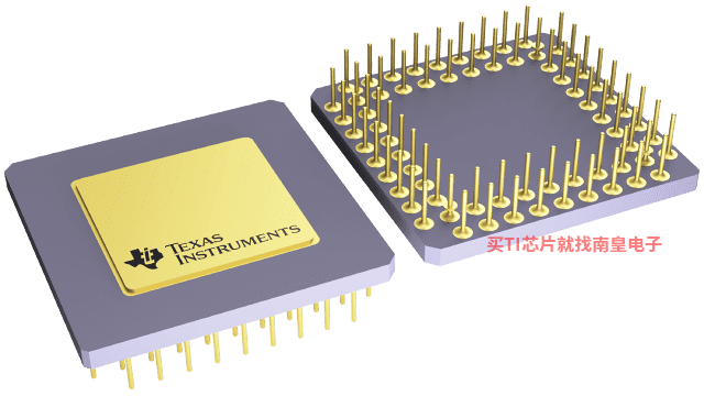
- Packaged in 44-Pin Plastic Leaded Chip Carrier (FN), 68-Pin Ceramic Pin Grid Array (GB), and 68-Pin Ceramic Quad Flat Packages (HV)
SCOPE and EPIC are trademarks of Texas Instruments Incorporated.
- Operating temperature range (C)
- -55 to 125
SN54ACT8990的完整型号有:5962-9322801MXA、5962-9322801MYA、SNJ54ACT8990GB、SNJ54ACT8990HV,以下是这些产品的关键参数及官网采购报价:
5962-9322801MXA,工作温度:-55 to 125,封装:CFP (HV)-68,包装数量MPQ:1个,MSL 等级/回流焊峰值温度:N/A for Pkg Type,引脚镀层/焊球材料:Call TI,TI官网5962-9322801MXA的批量USD价格:368.297(1000+)
5962-9322801MYA,工作温度:-55 to 125,封装:CPGA (GB)-68,包装数量MPQ:1个,MSL 等级/回流焊峰值温度:N/A for Pkg Type,引脚镀层/焊球材料:SNPB,TI官网5962-9322801MYA的批量USD价格:403.372(1000+)
SNJ54ACT8990GB,工作温度:-55 to 125,封装:CPGA (GB)-68,包装数量MPQ:1个,MSL 等级/回流焊峰值温度:N/A for Pkg Type,引脚镀层/焊球材料:SNPB,TI官网SNJ54ACT8990GB的批量USD价格:403.372(1000+)
SNJ54ACT8990HV,工作温度:-55 to 125,封装:CFP (HV)-68,包装数量MPQ:1个,MSL 等级/回流焊峰值温度:N/A for Pkg Type,引脚镀层/焊球材料:Call TI,TI官网SNJ54ACT8990HV的批量USD价格:368.297(1000+)

PSPICE-FOR-TI 适用于 TI 设计和模拟工具的 PSpice
PSpice for TI 可提供帮助评估模拟电路功能的设计和仿真环境。此功能齐全的设计和仿真套件使用 Cadence 的模拟分析引擎。PSpice for TI 可免费使用,包括业内超大的模型库之一,涵盖我们的模拟和电源产品系列以及精选的模拟行为模型。借助PSpice for TI 的设计和仿真环境及其内置的模型库,您可对复杂的混合信号设计进行仿真。创建完整的终端设备设计和原型解决方案,然后再进行布局和制造,可缩短产品上市时间并降低开发成本。
在PSpice for TI 设计和仿真工具中,您可以搜索 TI (...)
TINA-TI 基于 SPICE 的模拟仿真程序
TINA-TI 提供了 SPICE 所有的传统直流、瞬态和频域分析以及更多。TINA 具有广泛的后处理功能,允许您按照希望的方式设置结果的格式。虚拟仪器允许您选择输入波形、探针电路节点电压和波形。TINA 的原理图捕获非常直观 - 真正的“快速入门”。TINA-TI 安装需要大约 500MB。直接安装,如果想卸载也很容易。我们相信您肯定会爱不释手。
TINA 是德州仪器 (TI) 专有的 DesignSoft 产品。该免费版本具有完整的功能,但不支持完整版 TINA 所提供的某些其他功能。
如需获取可用 TINA-TI 模型的完整列表,请参阅:SpiceRack - 完整列表
需要 HSpice (...)